Solder-resisting photosensitive resin composition, printed wiring board and preparation technology of printed wiring board

A technology for printed circuit boards and photosensitive resins, which is applied in the photoengraving process of pattern surface, printed circuit, printed circuit manufacturing, etc. There are problems such as air bubbles and poor solder mask performance, achieving good exposure performance and thickness uniformity, shortening exposure time, and good mechanical properties.

Pending Publication Date: 2015-12-09
河北盈丰电子科技有限公司
View PDF5 Cites 6 Cited by
  • Summary
  • Abstract
  • Description
  • Claims
  • Application Information

AI Technical Summary

Problems solved by technology

[0005] One of the objectives of the present invention is to provide a solder resist photosensitive resin composition for preparing solder resist photosensitive dry films, so as to solve the problems of poor thermodynamic properties and poor mechanical properties of existing solder resist photosensitive dry films
[0006] The second object of the present i

Method used


Image

  • Solder-resisting photosensitive resin composition, printed wiring board and preparation technology of printed wiring board
  • Solder-resisting photosensitive resin composition, printed wiring board and preparation technology of printed wiring board
  • Solder-resisting photosensitive resin composition, printed wiring board and preparation technology of printed wiring board

Examples


Example Embodiment

[0033] Example 1

[0034] 1. Make solder mask photosensitive film

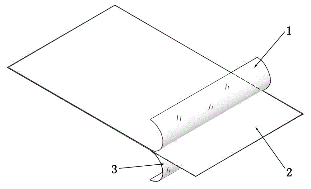
[0035] Such as figure 1 As shown, the prepared solder resist photosensitive dry film is composed of a three-layer structure of PE film 1, solder resist photosensitive dry film 2 and PET film 3. The specific manufacturing process is as follows:

[0036] a, weighing

[0037] Binder (polystyrene resin 10g, polystyrene resin 2g), epoxy resin (urethane modified epoxy resin 32g), monomer (pentaerythritol triacrylate 13g), photoinitiator (xylene ketone 13g), Additives (5g of phenylproprazole, 5g of triethylene glycol diacetate, 9g of polypropylene, 7g of ethylene (approximately equivalent to 5.6L)), dye (4g of malachite green).

[0038] b. Premix polystyrene, polystyrene resin, pentaerythritol triacrylate, dimethyl ketone, phenylproprazole, triethylene glycol diacetate, and polypropylene, and then add them to the polyurethane modified epoxy resin , The mixture is obtained, and then the mixture is shaken and stirred while dis...

Example Embodiment

[0055] Experimental example:

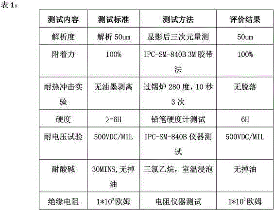
[0056] The performance of the dry film solder resist layer of the circuit boards prepared in Example 1 and Comparative Example 1 was tested and compared. The results are shown in Table 2 below:

[0057]

[0058] It can be seen from the comparison of the test item data in Table 2 that the solder mask formed by the UV curing method of the dry film of the present invention is superior to the thermal curing effect in terms of film thickness uniformity, resolution, and hardness.

Example Embodiment

[0059] Example 2

[0060] Compared with Example 1, the coating thickness in step c is 15 μm, and other conditions remain unchanged.


PUM

PropertyMeasurementUnit
Thicknessaaaaaaaaaa

Abstract

The invention discloses a solder-resisting photosensitive resin composition, a printed wiring board using a solder-resisting photosensitive dry film, prepared from the solder-resisting photosensitive resin composition, as a solder mask, and a preparation technology of the printed wiring board. The solder-resisting photosensitive resin composition comprises the following components: 11-13 wt% of a binder, 29-32 wt% of epoxy resin, 11-14 wt% of monomer, 12-14 wt% of a photoinitiator, 25-29 wt% of an additive and 3.5-4.5 wt% of dye. The solder-resisting photosensitive dry film prepared from the solder-resisting photosensitive resin composition disclosed by the invention has the following advantages: (1) the mechanical property is excellent: the dry film is thinner and higher in strength and has excellent heat shock resistance; (2) the curing speed is high: the photosensitive dry film requires short time of exposure, can particularly ensure the manufacturing accuracy of the printed wiring board, and is applicable to manufacture of high-density wired circuit boards; (3) the photosensitive dry film is attached to the printed wiring board through the function of pressure and temperature and adopts a specific manufacturing technology, and no bubble exists between the solder mask and the circuit board.

Description

technical field [0001] The invention relates to the production of printed circuit boards, in particular to a solder resist photosensitive resin composition, a printed circuit board with a dry film made of the composition as a solder resist layer and a manufacturing process thereof. Background technique [0002] There are usually three ways to make printed circuit board solder resist patterns. The screen plate directly prints the solder resist pattern, coats a photosensitive wet film to cure it to produce a solder resist pattern, or attaches a photosensitive dry film to develop and then cures to produce a solder resist pattern. Among them, the method of attaching a photosensitive dry film to develop a solder resist pattern is more suitable for circuit boards with high-density wiring, and can be accurately aligned with the wiring lines on the circuit board. Moreover, the dry film is not easy to contaminate the pad and affect the reliability of soldering. [0003] Although the...

Claims


Application Information

Patent Timeline
IPC IPC(8): G03F7/004G03F7/027H05K1/02H05K3/00
Inventor 张伯平
Owner 河北盈丰电子科技有限公司
Why Eureka
Try Eureka