Field effect diode and manufacturing method therefor

A technology of field effect diodes and manufacturing methods, applied in the direction of diodes, semiconductor/solid-state device manufacturing, electrical components, etc., can solve the problems of difficult control of the depth of trench etching, complicated manufacturing process, high turn-on voltage, etc., and achieve low reverse The effects of leakage current, simple manufacturing process, and low forward turn-on voltage

Active Publication Date: 2015-12-23
GPOWER SEMICON
View PDF4 Cites 2 Cited by
  • Summary
  • Abstract
  • Description
  • Claims
  • Application Information

AI Technical Summary

Problems solved by technology

[0006] The purpose of the present invention is to propose a field effect diode and its manufacturing method, which can solve the problems of high turn-on voltage, large reverse leakage, difficulty in controlling the depth of trench etching and complicated manufacturing process in the prior art

Method used


Image

  • Field effect diode and manufacturing method therefor
  • Field effect diode and manufacturing method therefor
  • Field effect diode and manufacturing method therefor

Examples


Embodiment 1

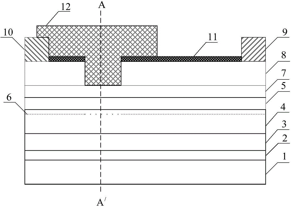
[0050] figure 1 It is a structural diagram of a field effect diode provided by Embodiment 1 of the present invention. Such as figure 1 As shown, the field effect diode consists of:

[0051] Substrate 1.

[0052] In this embodiment, the substrate material may be gallium nitride, silicon, sapphire or silicon carbide.

[0053] The nucleation layer 2 is located on the substrate 1 .

[0054] In this embodiment, the nucleation layer material may be aluminum nitride, gallium nitride or aluminum gallium nitride,

[0055] The buffer layer 3 is located on the nucleation layer 2 .

[0056] In this embodiment, the material of the buffer layer may be AlGaN or other III-V group compounds, and the thickness may be 1-3.5 microns.

[0057] The channel layer 4 is located on the buffer layer 3 .

[0058] In this embodiment, the material of the channel layer may be gallium nitride, and the thickness may be 15-35 nanometers.

[0059] The first barrier layer 5 is located on the channel layer ...

Embodiment 2

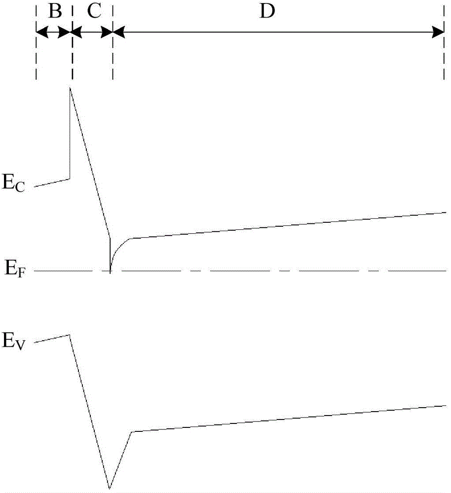
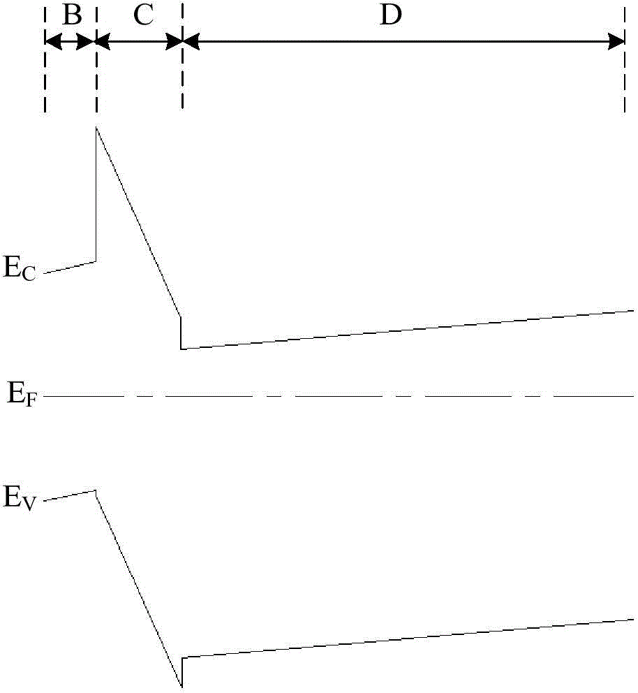
[0108] Figure 6 It is the structure diagram of the field effect diode provided by the second embodiment of the present invention. Such as Figure 6 As shown, different from the first embodiment of the present invention, the field effect diode provided by the second embodiment of the present invention further includes: a back barrier layer 13 located between the buffer layer 3 and the channel layer 4 .

[0109] In this embodiment, the material of the back barrier layer may be P-type GaN or P-type AlGaN. In this structure, the negative charge introduced by the P-type doping in the back barrier layer and the negative charge generated by the piezoelectric polarization further suppress the two-dimensional electron gas concentration in the channel layer, which can further regulate the turn-on voltage of the diode. , so as to obtain a turn-on voltage that is positive and close to 0V.

[0110] Figure 7 It is a flow chart of the manufacturing method of the field effect diode prov...

Embodiment 3

[0116] Figure 8 It is the structure diagram of the field effect diode provided by the third embodiment of the present invention. Such as Figure 8 As shown, different from the first embodiment of the present invention, the mass percentage of the aluminum component of the second barrier layer 8 of the field effect diode provided by the third embodiment of the present invention gradually decreases from top to bottom, and the shape of the trench is Inverted trapezoid.

[0117] In this embodiment, the mass percentage of the aluminum component of the second barrier layer gradually increases from bottom to top, showing a gradient change. During the thermal oxidation process of the second barrier layer, the degree of oxidation varies with the mass percentage of the aluminum component, and the higher the mass percentage of the aluminum component, the easier it is to be oxidized. Therefore, in the process of corroding and forming grooves, the part with a high mass percentage of alu...


PUM


Abstract

The invention discloses a field effect diode and a manufacturing method therefor. The field effect diode comprises a substrate, a channel layer located on the substrate, a first barrier layer located on the channel layer, an etching blocking layer located on the first barrier layer, a second barrier layer located on the etching blocking layer, a mask layer located on the second barrier layer, a groove located between the second barrier layer and the mask layer, a negative electrode located on the second barrier layer, and a positive electrode composed of Schottky electrodes located inside and outside the groove and a positive electrode ohmic contact electrode located on the second barrier layer in short circuit connection. The field effect diode has advantages of low forward cut-in voltage, low reverse leakage current and high breakdown voltage, the groove etching depth is easy to control, and the manufacturing technology is simple.

Description

technical field [0001] The invention relates to the technical field of semiconductors, in particular to a field effect diode and a manufacturing method thereof. Background technique [0002] The third-generation wide-bandgap semiconductor materials represented by GaN (gallium nitride) have excellent properties such as wide bandgap, high breakdown electric field strength, high saturation electron drift velocity, high thermal conductivity, and high concentration of two-dimensional electron gas at the heterogeneous interface. Compared with Si materials, GaN is more suitable for making power electronic devices with high power, high current density and high switching speed. Compared with traditional Si devices, GaN devices can carry higher power density and have higher energy conversion efficiency, which can reduce the volume and weight of the entire system, thereby reducing system cost. [0003] GaN-based Schottky barrier diodes can withstand a high reverse breakdown voltage, h...

Claims


Application Information

Patent Timeline
Patent Type & Authority Applications(China)
IPC IPC(8): H01L29/872H01L21/329
CPCH01L29/66212H01L29/872
Inventor 陈洪维裴轶
Owner GPOWER SEMICON
Why Eureka
Try Eureka