Silicon nano cone array coated with gold film as well as preparation method and application thereof

A silicon nanometer and cone array technology is applied in the fields of nanocone arrays and preparation, and can solve the problems that the product cannot be used for the detection of clenbuterol hydrochloride, the product cannot be obtained, the preparation method is complicated, and the production method is simple and convenient, and the preparation method is simple. , consistent and reproducible results

Inactive Publication Date: 2015-12-30
HEFEI INSTITUTES OF PHYSICAL SCIENCE - CHINESE ACAD OF SCI
View PDF5 Cites 19 Cited by
  • Summary
  • Abstract
  • Description
  • Claims
  • Application Information

AI Technical Summary

Problems solved by technology

But, no matter be product, or its preparation method, all there is weak point, at first, product can not be used for detecting clenbuterol hydrochloride; product

Method used


Image

  • Silicon nano cone array coated with gold film as well as preparation method and application thereof
  • Silicon nano cone array coated with gold film as well as preparation method and application thereof
  • Silicon nano cone array coated with gold film as well as preparation method and application thereof

Examples


Embodiment 1

[0037] The concrete steps of preparation are:

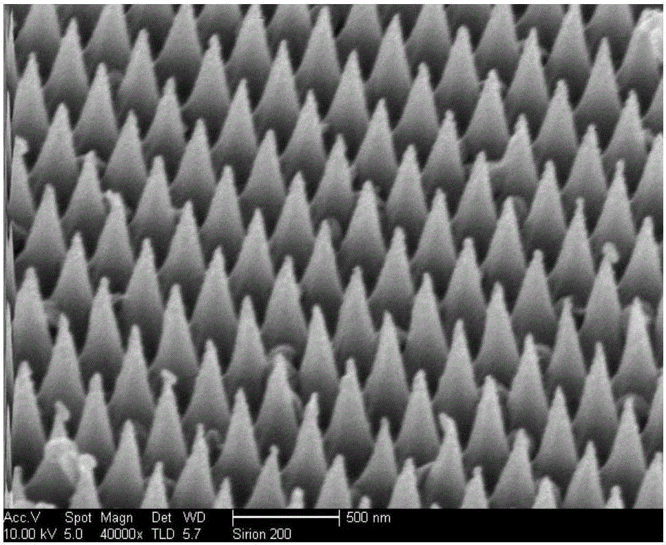
[0038] Step 1, first synthesize a single-layer colloidal crystal template with polystyrene colloidal spheres with a diameter of 250 nm on a silicon substrate through the gas-liquid interface self-assembly technology; Crystal silicon wafer. Then put the silicon substrate synthesized with a single-layer colloidal crystal template on it at a flow rate of 30 cm 3 / min and a pressure of 3.4Pa in a sulfur hexafluoride atmosphere for 3 minutes to obtain a silicon substrate with an ordered array of silicon nanocones placed thereon; wherein, the power of the plasma etching is 220W.

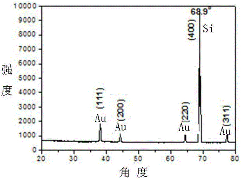
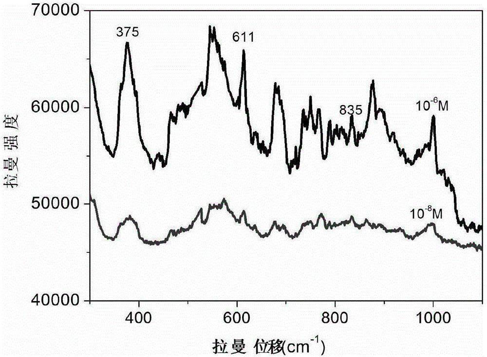
[0039] Step 2, using ion beam sputtering deposition (or thermal evaporation deposition) technology, depositing a gold film with a thickness of 15nm on a silicon substrate with an ordered array of silicon nanocones placed thereon; wherein, ion beam sputtering deposits a gold film When the deposition current is 18mA and the time is 5min, the obtained figure ...

Embodiment 2

[0041] The concrete steps of preparation are:

[0042] Step 1, first synthesize a single-layer colloidal crystal template with polystyrene colloidal spheres with a diameter of 280 nm on a silicon substrate through the gas-liquid interface self-assembly technology; Crystal silicon wafer. Then the silicon substrate synthesized with a single-layer colloidal crystal template is placed in a flow rate of 33 cm 3 / min and a pressure of 3.3Pa in a sulfur hexafluoride atmosphere for 3.3 minutes to obtain a silicon substrate with an ordered array of silicon nanocones; wherein, the power of the plasma etching is 210W.

[0043] Step 2, using ion beam sputtering deposition (or thermal evaporation deposition) technology, depositing a gold film with a thickness of 18nm on a silicon substrate with an ordered array of silicon nanocones placed thereon; wherein, the gold film is deposited by ion beam sputtering When the deposition current is 19mA and the time is 4.5min, the obtained figure 1 ...

Embodiment 3

[0045] The concrete steps of preparation are:

[0046] Step 1, first synthesize a single-layer colloidal crystal template with polystyrene colloidal spheres with a diameter of 300 nm on a silicon substrate through the gas-liquid interface self-assembly technology; Crystal silicon wafer. Place the silicon substrate on which the monolayer colloidal crystal template is synthesized at a flow rate of 35 cm 3 / min and a pressure of 3.2Pa in a sulfur hexafluoride atmosphere for 3.5 minutes to obtain a silicon substrate with an ordered array of silicon nanocones placed thereon; wherein, the power of the plasma etching is 200W.

[0047] Step 2, using ion beam sputtering deposition (or thermal evaporation deposition) technology, depositing a gold film with a thickness of 20nm on a silicon substrate with an ordered array of silicon nanocones placed thereon; wherein, ion beam sputtering deposits a gold film When the deposition current is 20mA and the time is 4min, the obtained figure 1 s...


PUM

PropertyMeasurementUnit
diameteraaaaaaaaaa
thicknessaaaaaaaaaa
wavelengthaaaaaaaaaa

Abstract

The invention discloses a silicon nano cone array coated with a gold film as well as a preparation method and an application thereof. The array is a silicon nano cone sequence array with a surface coated with a gold film, wherein the conical bottom diameter of silicon nano cones forming the silicon nano cone sequence array is 180nm to 220nm, the cone height is 450nm to 550nm, the cone period is 250nm to 350nm, and the thickness of the gold film is 15nm to 25nm. The preparation method comprises the following steps: first synthesizing polystyrene colloidal spheres on a silicon substrate to form a single-layer colloidal crystal template by virtue of a gas-liquid interface self-assembling technology, placing the silicon substrate with the single-layer colloidal crystal template in a sulfur hexafluoride atmosphere, etching the silicon substrate by virtue of plasma to obtain the silicon substrate with silicon nano cone sequence array, and depositing the gold film on the silicon substrate with the silicon nano cone sequence array by utilizing an ion beam sputtering technology or thermal evaporation deposition technology to obtain a target product. The silicon nano cone array can be used as an active substrate of surface enhanced raman scattering to measure the content of clenbuterol hydrochloride attached thereon.

Description

technical field [0001] The invention relates to a nanocone array, its preparation method and application, in particular to a silicon nanocone array coated with a gold film, its preparation method and application. Background technique [0002] Molecular structure is Clenbuterol hydrochloride, commonly known as clenbuterol. If clenbuterol hydrochloride is used in the process of raising animals artificially, although it can reduce the formation of animal fat and improve the conversion efficiency of lean meat, it will cause the clenbuterol hydrochloride molecule to remain in the animal body for a long time. If people eat meat containing clenbuterol, they will experience symptoms of poisoning such as dizziness, palpitations, and numb fingers. At present, the commonly used methods for detecting clenbuterol hydrochloride include gas chromatography-mass spectrometry, high performance liquid chromatography, mold labeling immunosorbent assay, capillary electrophoresis, etc., but al...

Claims


Application Information

Patent Timeline
Patent Type & Authority Applications(China)
IPC IPC(8): B82B1/00B82B3/00B82Y30/00B82Y40/00G01N21/65
Inventor 刘广强赵倩蔡伟平
Owner HEFEI INSTITUTES OF PHYSICAL SCIENCE - CHINESE ACAD OF SCI
Why Eureka
Try Eureka