
Aluminum oxide-gallium oxide mixed-crystal material for wide-band-gap semiconductors

A wide bandgap semiconductor, alumina technology, applied in the growth of polycrystalline materials, single crystal growth, inorganic chemistry and other directions, can solve the problems of low doping concentration, poor material quality, difficult growth technology, etc., to achieve uniform color, High optical quality effect

Inactive Publication Date: 2016-01-13
SHANGHAI INST OF OPTICS & FINE MECHANICS CHINESE ACAD OF SCI
View PDF2 Cites 7 Cited by
  • Summary
  • Abstract
  • Description
  • Claims
  • Application Information

AI Technical Summary

Problems solved by technology

[0006] (1) In order to meet the requirements for the light transmittance of the substrate, deep ultraviolet LED materials usually have to be grown on substrates such as sapphire and AlN, and the heterogeneous epitaxial growth technology of materials is generally too difficult, resulting in generally poor material quality;
[0007] (2) In order to achieve deep ultraviolet luminescence, the Al component content of the active layer AlGaN should usually reach 45%-50%. AlGaN materials with high aluminum components still have the problem of low doping concentration, which also causes the electro-optic conversion efficiency of deep ultraviolet LEDs. Main reason for generally low (1-2%)
[0008] After more than ten years of development, although some progress has been made, overall, the deep ultraviolet LED technology based on the GaN system is far from mature

Method used


Image

  • Aluminum oxide-gallium oxide mixed-crystal material for wide-band-gap semiconductors
  • Aluminum oxide-gallium oxide mixed-crystal material for wide-band-gap semiconductors

Examples


Embodiment 1

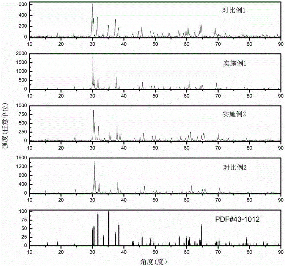
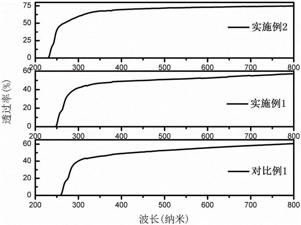
[0029] The aluminum oxide-gallium oxide mixed crystal material is grown by using the above-mentioned raw material ratio and process flow, and x=0.1 is taken in the raw material ratio. Ga 2 o 3 , Al 2 o 3 High-purity raw materials (all with a purity of 99.999%) are weighed in a molar ratio of 0.9:0.1. The raw materials were mixed evenly by ethanol wet ball milling for 16 hours, baked in an oven at 100°C for 6 hours, pressed into a rod with an organic elastic plastic mold in an isostatic press, and sintered in a muffle furnace at 1500°C for 10 hours. Put the sintered material rod into the floating zone furnace as the upper rod, and the gallium oxide seed crystal as the lower rod. The temperature rises to melt and inoculate the seed crystals, starting crystal growth. The crystal growth rate was 5 mm / h, the rotation rate was 10 rpm, and the atmosphere was air. After the crystal growth was completed, the melting zone was pulled off, and the temperature was slowly lowered to r...

Embodiment 2

[0031] The aluminum oxide-gallium oxide mixed crystal material is grown by using the above-mentioned raw material ratio and process flow, and x=0.3 is taken in the raw material ratio. Ga 2 o 3 , Al 2 o 3 High-purity raw materials (all with a purity of 99.999%) are weighed in a molar ratio of 0.7:0.3. The raw materials were mixed evenly by ethanol wet ball milling for 18 hours, baked in an oven at 70°C for 10 hours, pressed into a rod with an organic elastic plastic mold in an isostatic press, and sintered in a muffle furnace at 1500°C for 10 hours. Put the sintered material rod into the floating zone furnace as the upper rod, and the gallium oxide seed crystal as the lower rod. The temperature rises to melt and inoculate the seed crystals, starting crystal growth. The crystal growth rate was 4 mm / h, the rotation rate was 12 rpm, and the atmosphere was air. After the crystal growth was completed, the melting zone was pulled off, and the temperature was slowly lowered to r...


PUM


Abstract

The invention relates to an aluminum oxide-gallium oxide mixed-crystal material for wide-band-gap semiconductors and a preparation method therefor. The structural formula of the aluminum oxide-gallium oxide mixed-crystal material is Ga(2-2x)Al2xO3, wherein the mole ratio x of doped aluminum oxide is 0-50%. According to the aluminum oxide-gallium oxide mixed-crystal material for the wide-band-gap semiconductors and the preparation method therefor, a mixed crystal is formed in a manner of maintaining the original gallium oxide crystal structure, has very high optical quality, is free of defects such as cracking, scattering particles and bubbles and is uniform in color; and through doping, the ultraviolet absorption cutoff edge of the ultraviolet absorption cutoff edge extends to 210-255nm, so that the aluminum oxide-gallium oxide mixed-crystal material is a very excellent deep-ultraviolet substrate material.

Description

technical field [0001] The invention relates to the field of artificial crystals, in particular to an aluminum oxide-gallium oxide mixed crystal material used for wide bandgap semiconductors. Background technique [0002] β-Ga 2 o 3 It is a wide bandgap compound semiconductor material with a direct bandgap. The bandgap width is about 4.8-4.9eV. It is the transparent conductive material with the widest bandgap known so far. It has many advantages such as large band gap, high breakdown field strength, fast saturated electron drift speed, small dielectric constant, high thermal conductivity, stable chemical properties, etc. It is transparent from ultraviolet to visible light bands, compared with traditional transparent Conductive materials (TCOs) can be used to fabricate a new generation of semiconductor optoelectronic devices operating in the shorter wavelength range. [0003] β-Ga 2 o 3 The material can be used as the substrate material of GaN. It has both the high trans...

Claims


Application Information

Patent Timeline
IPC IPC(8): C30B29/22C30B13/00C01G15/00
Inventor 夏长泰赛青林肖海林
Owner SHANGHAI INST OF OPTICS & FINE MECHANICS CHINESE ACAD OF SCI
Learn More