Fd-goi tunneling field-effect transistor with abrupt tunneling junction and preparation method thereof
A tunneling field effect and tunneling junction technology, used in semiconductor/solid-state device manufacturing, diodes, semiconductor devices, etc., can solve the problems of small driving current and sub-threshold slope theoretical value degradation, achieve low parasitic capacitance, suppress dual Pole effect, effect with high tunneling probability
- Summary
- Abstract
- Description
- Claims
- Application Information
AI Technical Summary
Problems solved by technology
Method used
Image
Examples
Embodiment 1
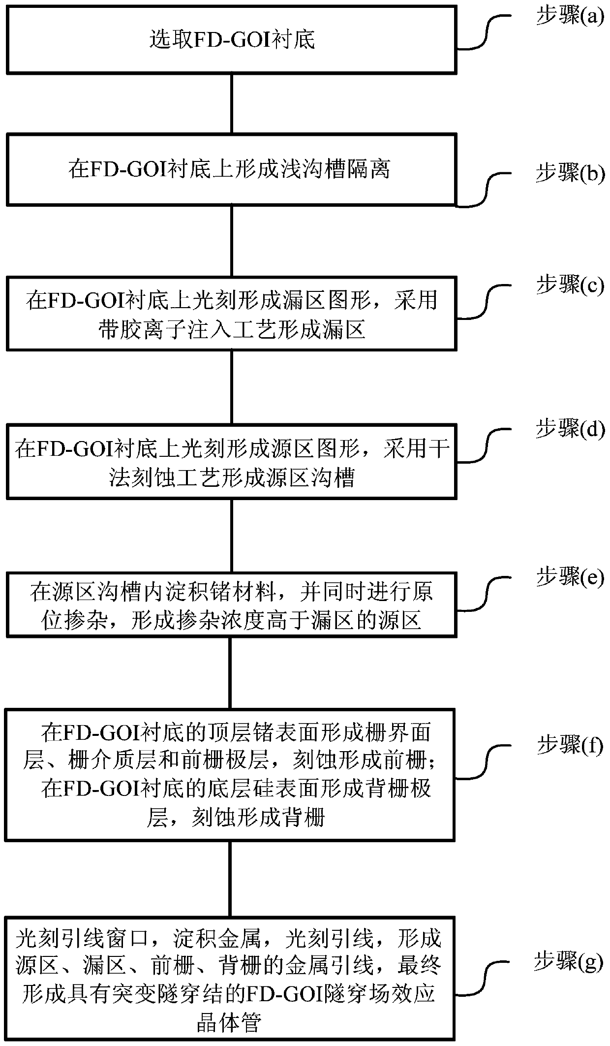
[0055] See figure 1 , figure 1 It is a flowchart of a method for preparing an FD-GOI tunneling field effect transistor with a sudden tunnel junction according to an embodiment of the present invention, and the method includes the following steps:
[0056] Step (a), selecting a fully depleted germanium-on-insulator (Fully Depleted Germanium-On-Insulator, referred to as FD-GOI) substrate;
[0057] Step (b), forming shallow trench isolation on the FD-GOI substrate by an etching process;
[0058] Step (c), forming a drain region pattern by photolithography on the FD-GOI substrate, and forming a drain region by using an ion implantation process with glue;
[0059] Step (d), forming a source region pattern by photolithography on the FD-GOI substrate, and forming a source region trench by a dry etching process;
[0060] Step (e), depositing germanium material in the trench of the source region, and performing in-situ doping at the same time, forming a source region with a higher...
Embodiment 2
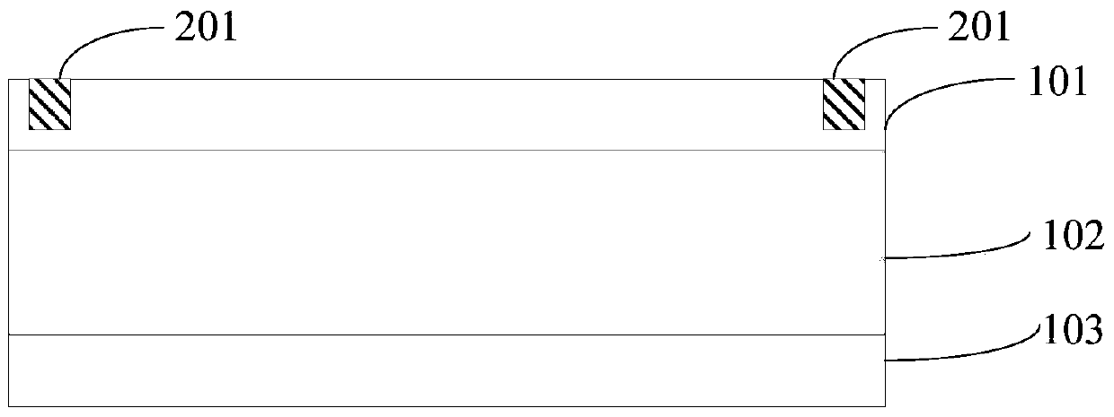
[0095] See Figure 2a-Figure 2h It is a schematic diagram of a method for preparing a FD-GOI tunneling field-effect transistor with a sudden tunnel junction according to an embodiment of the present invention; the specific steps are as follows:
[0096] (1) Select the FD-GOI substrate. Such as Figure 2a As shown, the FD-GOI substrate includes a top layer of germanium 101 , a buried oxide layer 102 such as a buried layer of silicon dioxide, and a bottom layer of silicon 103 .
[0097] The reason for using the FD-GOI substrate is that the Ge material has a small bandgap, high tunneling probability, high carrier mobility, and good velocity characteristics, which is conducive to improving the driving current of the tunneling field effect transistor; the GOI substrate formed Semiconductor devices have the advantages of low power consumption, high speed, high integration density, strong anti-interference ability, strong anti-irradiation ability, and simple process, which can prov...
Embodiment 3
[0127] See image 3 , image 3 It is a schematic flow chart of a method for preparing an FD-GOI tunneling field effect transistor with an abrupt tunneling junction according to an embodiment of the present invention, so as to prepare an N-type FD-GOI tunneling field effect transistor with an abrupt tunneling junction with a channel length of 45 nm. Taking the transistor as an example to describe in detail, the specific steps are as follows:
[0128] 1. Select FD-GOI substrate
[0129] The crystal orientation of the FD-GOI substrate can be (100) or (110) or (111), without any limitation here. In addition, the doping type of the FD-GOI substrate 101 can be N-type or It is P-type, and the doping concentration is, for example, 10 14 ~10 17 cm -3 , the thickness of the top Ge layer is, for example, 20-100 nm, preferably 20 nm.
[0130] 2. Shallow trench isolation formation
[0131] 2.1 Form the first protective layer on the FD-GOI substrate.
[0132] First, two layers of mate...
PUM
 Abstract
Description
Claims
Application Information
 - R&D
- Intellectual Property
- Life Sciences
- Materials
- Tech Scout
- Unparalleled Data Quality
- Higher Quality Content
- 60% Fewer Hallucinations
Browse by: Latest US Patents, China's latest patents, Technical Efficacy Thesaurus, Application Domain, Technology Topic, Popular Technical Reports.
© 2025 PatSnap. All rights reserved.Legal|Privacy policy|Modern Slavery Act Transparency Statement|Sitemap|About US| Contact US: help@patsnap.com


