Gridless AlGaN/GaN field effect transistor sensor, and preparation method thereof

A field effect transistor and sensor technology, applied in the field of gateless AlGaN/GaN field effect transistor sensor and its preparation, can solve the problems of difficulty in identification of pollutants, difficulty in detection of pollutants, etc., and achieves improved selective adsorption, convenient and rapid reuse , the effect of high-precision quantitative detection

Active Publication Date: 2016-02-03
NANJING UNIV
View PDF3 Cites 9 Cited by
  • Summary
  • Abstract
  • Description
  • Claims
  • Application Information

AI Technical Summary

Problems solved by technology

The problem of water pollution has attracted more and more people's attention. Effective detection of water pollutants has become

Method used


Image

  • Gridless AlGaN/GaN field effect transistor sensor, and preparation method thereof
  • Gridless AlGaN/GaN field effect transistor sensor, and preparation method thereof
  • Gridless AlGaN/GaN field effect transistor sensor, and preparation method thereof

Examples


Embodiment 1

[0045] Realization of Po 4 3- ion detection as an example.

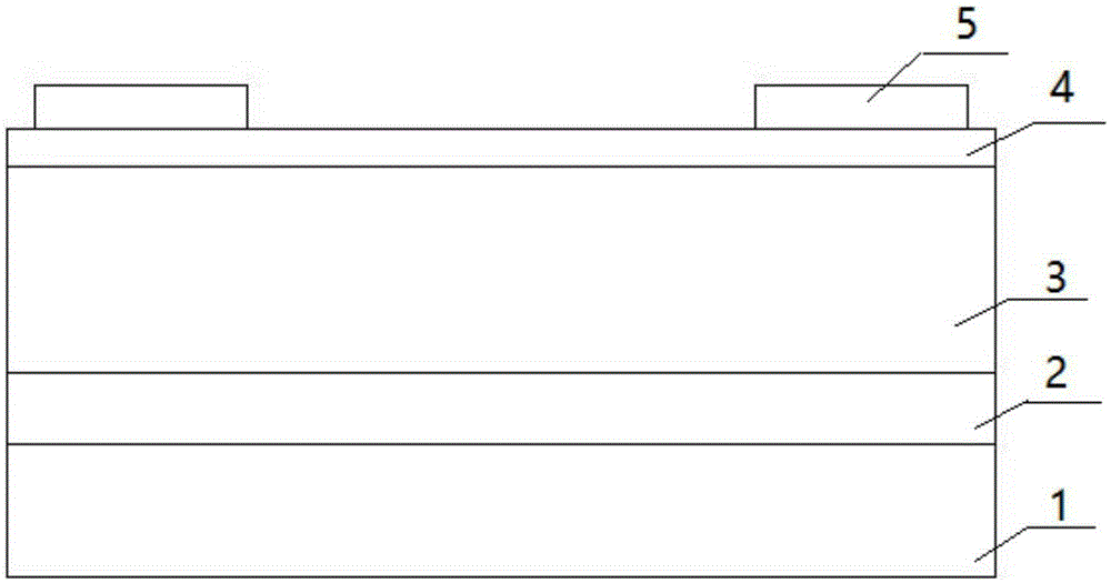
[0046] (1) First, the preparation steps of AlGaN / GaN heterojunction materials:

[0047] 1. A thin AlN nucleation layer of 22nm is grown on the SiC substrate 1;

[0048] 2. Then grow a thick GaN buffer layer of 32um;

[0049] 3. Finally, a 25nm AlGaN barrier layer 4 is grown, and the Al composition of the AlGaN thin film is 0.3.

[0050] The second is the preparation process steps of AlGaN / GaN field effect transistor sensor:

[0051] (2) substrate cleaning, first with 50% hydrochloric acid, 50% KOH each treatment for 10 minutes, remove the oxide layer on the surface, rinse repeatedly with deionized water, acetone, alcohol, deionized water in order to ultrasonic 10 minutes;

[0052] (3) Ohmic contact electrodes, on the cleaned AlGaN / GaN heterogeneous crystal sheet, use electron beam evaporation technology to deposit the source electrode 51, the source electrode PAD52 connected to the source electrode, the drain el...

Embodiment 2

[0073] AlGaN / GaN field-effect transistor sensors prepared on sapphire substrate 3 CCOO - ion detection as an example.

[0074] 1. First, the preparation steps of AlGaN / GaN heterojunction materials:

[0075] Method is with embodiment 1. the difference lies in:

[0076] 1. Grow a thin AlN nucleation layer of 1nm on a sapphire substrate;

[0077] 2. Then grow a thick GaN buffer layer 1um;

[0078] 3. Finally, a 15nm AlGaN barrier layer is grown, and the Al composition of the AlGaN film is 0.2.

[0079] Second, the second is the preparation process steps of AlGaN / GaN field effect transistor sensor:

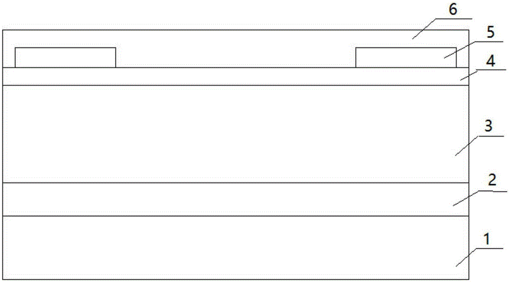
[0080] 1. Substrate cleaning; 2. Ohmic contact electrodes; 3. Making SiO 2 Passivation layer, passivation method is with embodiment 1;

[0081] 4. The surface of the gate-free area is functionalized. Firstly, the gate-free area is oxidized by inductively coupled plasma etching (ICP); 2 Blow dry; then put the substrate into r-aminopropyltrimethoxysilane (AMPS) aqueous solution...

Embodiment 3

[0094] Realization of Cr 2 o 4 2- ion detection as an example.

[0095] 1. First, the preparation steps of AlGaN / GaN heterojunction materials:

[0096] Method is with embodiment 1. the difference lies in:

[0097] 1. Growth of a thin AlN nucleation layer of 3nm on a SiC substrate;

[0098] 2. Then grow a thick GaN buffer layer of 3um;

[0099] 3. Finally, a 20nm AlGaN barrier layer is grown, and the Al composition of the AlGaN film is 0.22.

[0100] Second, the second is the preparation process steps of AlGaN / GaN field effect transistor sensor:

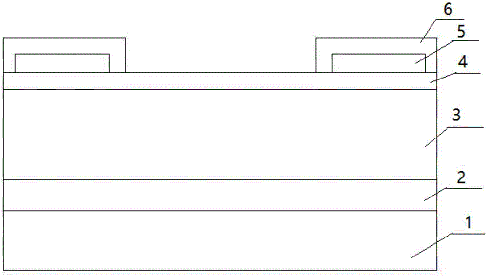
[0101] 1. substrate cleaning; 2. ohmic contact electrode; 3. passivation method with embodiment 1

[0102] 4. The surface of the gate-free area is functionalized. Firstly, the gate-free area is oxidized by inductively coupled plasma etching (ICP); 2 Blow dry; then put the substrate into r-aminopropyltrimethoxysilane (AMPS) aqueous solution (V AMPS :V H2O =1:10) React at 50°C for 24h, put it in a vacuum oven and dry at 120°C...


PUM

PropertyMeasurementUnit
Thicknessaaaaaaaaaa
Thicknessaaaaaaaaaa
Thicknessaaaaaaaaaa

Abstract

The invention provides a gridless AlGaN/GaN field effect transistor sensor. According to the gridless AlGaN/GaN field effect transistor sensor, electrodes are arranged on an AlGaN/GaN heterojunction substrate via vapor deposition; the gridless AlGaN/GaN field effect transistor sensor also comprises a passivation layer; a whole source end electrode, a source end electrode PAD, a leakage end electrode, and a leakage end electrode PAD are covered by the passivation layer; the passivation layer used for covering the source end electrode PAD and the leakage end electrode PAD is provided with windows via etching until the PADs are exposed; the gridless AlGaN/GaN field effect transistor sensor also comprises an ion imprinted polymer layer, the ion imprinted polymer layer is arranged on an AlGaN layer, and possesses imprinting holes. The invention also discloses a preparation method of the gridless AlGaN/GaN field effect transistor sensor. The conductive polymer nano composite material possesses single ion identification performance, is capable of improving selective adsorption and anti-interference performance of devices, is capable of realizing quick response and high accuracy quantitative determination, can be reused conveniently and quickly after washing with NaCl solution, is convenient to use, is low in cost, and can be used for water quality on-line monitoring.

Description

technical field [0001] The patent of the invention relates to the field of environmental detection, in particular to a gateless AlGaN / GaN field-effect transistor sensor with ion recognition and concentration detection and its preparation method. Background technique [0002] Molecularly imprinted polymer (MIP) is a new technology that has emerged in recent years to prepare polymers with recognition functions for template molecules. , biosensors, selective catalysis and other fields have shown superiority, which has become one of the research hotspots. The problem of water pollution has attracted more and more people's attention. Effective detection of water pollutants has become one of the important issues closely related to people's daily life. It is difficult to realize the identification of pollutants. [0003] In view of the above situation, the present invention proposes a new type of gateless AlGaN / GaN field effect transistor sensor for detecting harmful Anions, the...

Claims


Application Information

Patent Timeline
IPC IPC(8): G01N27/414
Inventor 陈敦军贾秀玲张荣郑有炓
Owner NANJING UNIV
Why Eureka
Try Eureka