Surface-processed copper foil, copper foil with carrier, laminated body, printed circuit board, electronic equipment, manufacturing method for surface-processed copper foil and manufacturing method for printed circuit board
A technology of surface treatment layer and copper foil with carrier, which is applied in the direction of printed circuit manufacturing, printed circuit, printed circuit, etc., and can solve problems such as silane condensation, reduced peel strength, and mismatching production steps of double-layer flexible printed wiring boards.
- Summary
- Abstract
- Description
- Claims
- Application Information
AI Technical Summary
Problems solved by technology
Method used
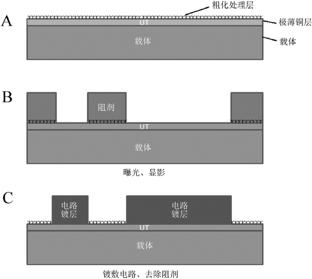
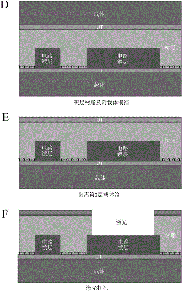
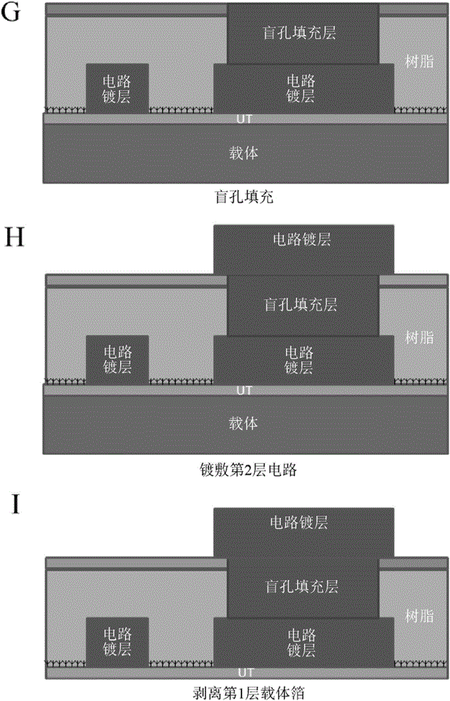
Image

Examples
Embodiment 12
[0217]
[0218] (1) Ni layer (Ni plating)
[0219] The carrier was electroplated using a roll-to-roll type continuous plating line under the following conditions, thereby forming a 1000 μg / dm 2 The amount of Ni layer attached. The specific plating conditions are described below.
[0220] Nickel sulfate: 270~280g / L
[0221] Nickel chloride: 35~45g / L
[0222] Nickel acetate: 10~20g / L
[0223] Boric acid: 30~40g / L
[0224] Gloss agent: saccharin, butynediol, etc.
[0225] Sodium lauryl sulfate: 55~75ppm
[0226] pH value: 4~6
[0227] Bath temperature: 55~65℃
[0228] Current density: 10A / dm 2
[0229] (2) Cr layer (electrolytic chromate treatment)
[0230] Next, after washing and pickling the surface of the Ni layer formed in (1), continue on the roll-to-roll type continuous plating line, and make 11 μg / dm by electrolytic chromate treatment under the following conditions. 2 The amount of Cr layer attached to the Ni layer.
[0231] Potassium dichromate 1~10g / L, zin...
Embodiment 13
[0249]
[0250] (1) Ni-Mo layer (nickel-molybdenum alloy plating)
[0251] The carrier was electroplated using a roll-to-roll type continuous plating line under the following conditions, thereby forming a 3000 μg / dm 2 The attached amount of Ni-Mo layer. The specific plating conditions are described below.
[0252] (Liquid composition) Ni sulfate hexahydrate: 50g / dm 3 , Sodium molybdate dihydrate: 60g / dm 3 , Sodium citrate: 90g / dm 3
[0253] (Liquid temperature) 30°C
[0254] (current density) 1~4A / dm 2
[0255] (power-on time) 3 to 25 seconds
[0256]
[0257] An ultra-thin copper layer is formed on the Ni-Mo layer formed in (1). The ultra-thin copper layer was formed on the same conditions as in Example 12 except that the thickness of the ultra-thin copper layer was 2 μm.
Embodiment 14
[0259]
[0260] (1) Ni layer (Ni plating)
[0261] The Ni layer was formed under the same conditions as in Example 12.
[0262] (2) Organic layer (organic layer formation process)
[0263] Next, after washing and pickling the surface of the Ni layer formed in (1), continue under the following conditions to rinse and spray the Ni layer surface for 20 to 120 seconds with a liquid temperature of 40°C and a pH of 5. An aqueous solution, thereby forming an organic layer, the aqueous solution containing carboxybenzotriazole (CBTA) at a concentration of 1 to 30 g / L.
[0264]
[0265] An ultra-thin copper layer is formed on the organic layer formed in (2). The ultra-thin copper layer was formed on the same conditions as in Example 12 except that the thickness of the ultra-thin copper layer was 3 μm.
PUM
| Property | Measurement | Unit |
|---|---|---|
| Current density | aaaaa | aaaaa |
| Current density | aaaaa | aaaaa |
| Thickness | aaaaa | aaaaa |
Abstract
Description
Claims
Application Information
 - R&D
- Intellectual Property
- Life Sciences
- Materials
- Tech Scout
- Unparalleled Data Quality
- Higher Quality Content
- 60% Fewer Hallucinations
Browse by: Latest US Patents, China's latest patents, Technical Efficacy Thesaurus, Application Domain, Technology Topic, Popular Technical Reports.
© 2025 PatSnap. All rights reserved.Legal|Privacy policy|Modern Slavery Act Transparency Statement|Sitemap|About US| Contact US: help@patsnap.com