MEMS micro array structure processing method based on micro-electroplating

A technology of micro-array and processing technology, which is applied in the direction of technology for producing decorative surface effects, micro-structure technology, micro-structure devices, etc., and can solve problems such as poor adhesion and uneven coating metal

Inactive Publication Date: 2016-02-17
SHANGHAI NORMAL UNIVERSITY
View PDF5 Cites 10 Cited by
  • Summary
  • Abstract
  • Description
  • Claims
  • Application Information

AI Technical Summary

Problems solved by technology

The invention solves the problems of uneven coating metal and poor adhesi

Method used


Image

  • MEMS micro array structure processing method based on micro-electroplating
  • MEMS micro array structure processing method based on micro-electroplating
  • MEMS micro array structure processing method based on micro-electroplating

Examples


Embodiment Construction

[0011] Below in conjunction with accompanying drawing and embodiment the present invention will be further described

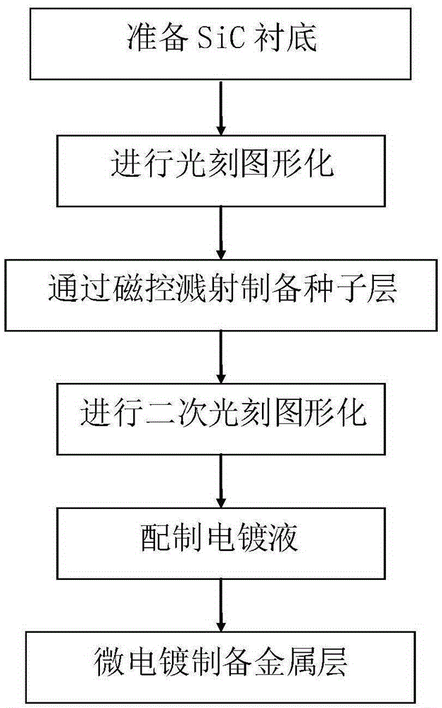
[0012] A kind of MEMS micro-array structure processing process based on micro-electroplating of the present invention (such as figure 1 shown), including the following steps:

[0013] Step 1, preparing the SiC substrate: the substrate is a SiC wafer, polished on both sides, and cleaned by RCA.

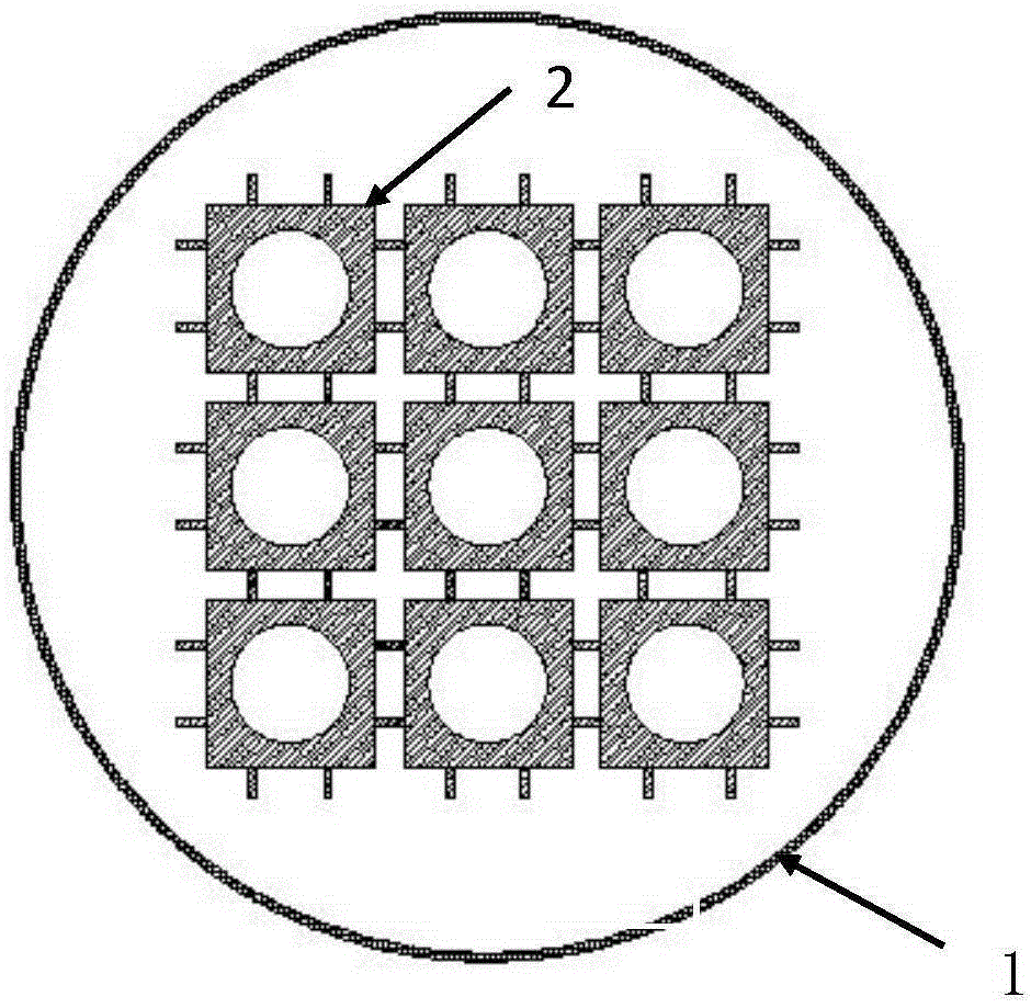
[0014] Step 2, carry out photolithography patterning, use Unicom microstructure (such as figure 2 shown), 1 in the accompanying drawings is a SiC wafer, and 2 is a Unicom microstructure.

[0015] On the wafer 1, evenly coat a photoresist of about 1-5 μm with a glue leveler, place it on a glue baking table at a temperature of 100°C for 3 minutes, and use a UV photolithography machine to expose it for 50 seconds, and develop it for 40 seconds. Put it on the rubber baking table for 10min to harden the film.

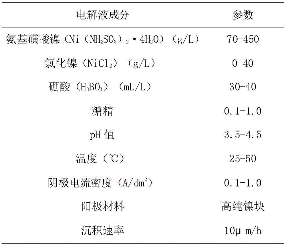
[0016] Step 3, prepare the seed layer: put the patterned s...


PUM


Abstract

The invention discloses a MEMS micro array structure processing method based on micro-electroplating, and more specifically relates to a mask preparation method via semiconducting material deep etching processing, and belongs to the technical field of semiconducting material processing. A SiC material is taken as an example. The MEMS micro array structure processing method comprises following steps: SiC substrate preparation; photoetching pattern forming; seed layer preparation via magnetron sputtering; secondary photoetching pattern forming; preparation of an electroplate liquid; and preparation of metal layers via electroplating. A electroplate liquid component is optimized, micro electroplating conditions are modified, adhesive force of a coated metal with a substrate is increased, uniformity and thickness of the coated metal are increased, and a prepared metal coating is capable of satisfying requirements of SiC deep etching processing of a mask layer, and expanding applications of silicon carbide in related device preparation via a novel mask structure. The MEMS micro array structure processing method is capable of providing technical supports for applications of SiC pressure sensors at severe environments (high temperature, high pressure, strong corrosion, and strong radiation).

Description

technical field [0001] The invention relates to the technical field of semiconductor material processing, in particular to a method for preparing a deep etching processing mask and metallization of a semiconductor material with corrosion resistance, stable chemical properties and high mechanical strength. Background technique [0002] MEMS are micron-sized mechanical systems, typically ranging in size from microns to millimeters. It refers to a micro-device or system that can be mass-produced and integrates micro-mechanisms, micro-sensors, micro-actuators, and signal processing and control circuits, up to interfaces, communications, and power supplies. MEMS is developed with the development of semiconductor integrated circuit microprocessing technology and ultra-precision machining technology. It is generally manufactured by similar semiconductor technology, such as surface micromachining, body micromachining and other technologies. It has the advantages of small size, ligh...

Claims


Application Information

Patent Timeline
IPC IPC(8): B81C1/00C23C28/02C23C14/35C23C14/04C23C14/18C25D3/12C25D5/02
CPCB81C1/00531B81C1/00373B81C1/00388B81C1/00595B81C1/00849B81C2201/01C23C14/04C23C14/185C23C14/35C23C28/023C25D3/12C25D5/024
Inventor 赵高杰孙玉俊刘益宏廖黎明刘少雄李星月姜舒月陈之战
Owner SHANGHAI NORMAL UNIVERSITY
Why Eureka
Try Eureka