High voltage LED chip preparation method being able to form isolated slot through scribing and corrosion

An LED chip and isolation groove technology, applied in the field of optoelectronics, can solve the problems of complex process flow, short-circuit failure, complex preparation process, etc., and achieve the effect of simplifying the process flow, solving short-circuit failure and simple process

Inactive Publication Date: 2016-02-17
SHANDONG INSPUR HUAGUANG OPTOELECTRONICS
View PDF6 Cites 5 Cited by
  • Summary
  • Abstract
  • Description
  • Claims
  • Application Information

AI Technical Summary

Problems solved by technology

However, its preparation process is complicated
[0006] In summary, although the existing technology solves the problems of short-circuit failure and low turn-on voltage caused by the formation of isolation grooves by ICP etching for high-voltage LEDs, it still has disadvantages such as complicated process flow and poor controllability.

Method used


Image

  • High voltage LED chip preparation method being able to form isolated slot through scribing and corrosion
  • High voltage LED chip preparation method being able to form isolated slot through scribing and corrosion

Examples


Embodiment Construction

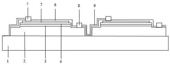
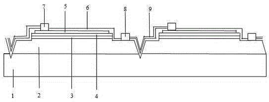
[0029] The high-voltage LED chip in the present invention, such as figure 2 As shown, it includes a sapphire substrate 1, an n-type GaN layer 2, a quantum well layer 3, a p-type GaN layer 4, an ITO transparent conductive film layer 5 and a passivation layer 6 arranged from bottom to top. Layer 5, n-type GaN layer 2 and passivation layer 6 are respectively provided with p-electrode 7, n-electrode 8 and metal lead 9.

[0030] The preparation method of the above-mentioned high-voltage LED chip comprises the following steps:

[0031] (1) In the reaction chamber of the metal-organic chemical vapor deposition equipment, the n-type GaN layer 2, the quantum well layer 3 and the p-type GaN layer 4 are sequentially grown on the substrate 1 to obtain a GaN-based epitaxial wafer. Substrate 1 may be sapphire, SiC or silicon.

[0032] (2) Use the existing ICP dry etching method to etch the mesa structure along the p-type GaN layer 4 to the n-type GaN layer 2 of the GaN-based epitaxial wa...


PUM


Abstract

The invention provides a high voltage LED chip preparation method being able to form an isolated slot through scribing and corrosion. The preparation method comprises the steps: 1) obtaining a GaN-based epitaxial wafer; 2) etching out an N type mesa structure; 3) forming a protective layer on the surface of the epitaxial wafer; 4) scribing to a substrate along the N type mesa through a laser scribing machine to obtain a wafer; 5) performing high temperature corrosion for the wafer, removing the protective layer, and forming an isolated slot; 6) forming a transparent conducting layer on the surface of a p type GaN layer; 7) making a passivation layer; 8) preparing a P electrode, an N electrode and a metal leading wire which connects two grains; and 9) obtaining a high voltage LED chip after thinning the wafer and scribing the wafer with cracks. The high voltage LED chip preparation method can form the isolated slot through laser scribing and high temperature corrosion, and not only solves the problem that an existing high voltage chip is short circuit and loses efficacy and the starting voltage is low and adverse, but also has the advantages of being simple in process and high in yield rate. Besides, as laser scribing is performed, wafer cracking can be directly performed after being thinned and the subsequent technological process can be simplified.

Description

technical field [0001] The invention relates to a method for preparing a high-voltage LED (light-emitting diode) chip by scribing and corroding to form an isolation groove, and belongs to the field of optoelectronic technology. Background technique [0002] In recent years, LED has gradually become one of the most valued light source technologies. On the one hand, LED has the characteristics of small size; on the other hand, LED has the power-saving characteristics of low current and low voltage drive; at the same time, it also has many advantages such as firm structure, strong shock and earthquake resistance, and long life. Among them, as one of the main applications in the field of optoelectronics, GaN-based materials have attracted more and more attention. GaN-based semiconductor materials can be used to produce ultra-high brightness blue, green, and white light-emitting diodes. In recent years, various technologies have emerged to improve the luminous brightness of LEDs...

Claims


Application Information

Patent Timeline
Patent Type & Authority Applications(China)
IPC IPC(8): H01L33/00
CPCH01L33/0075
Inventor 吴向龙彭璐刘琦王成新徐现刚
Owner SHANDONG INSPUR HUAGUANG OPTOELECTRONICS
Why Eureka
Try Eureka