Preparation method of p-type tin dioxide thin film capable of realizing near-band-edge ultraviolet luminescence

A technology of tin dioxide and thin film, which is applied in the field of preparation of p-type SnO2 thin film, can solve the problems of low solid solubility, reduce acceptor ionization energy, etc., and achieve the effect of improving solid solubility

Inactive Publication Date: 2017-08-29
JILIN UNIV
View PDF2 Cites 0 Cited by
  • Summary
  • Abstract
  • Description
  • Claims
  • Application Information

AI Technical Summary

Problems solved by technology

[0003] The purpose of the present invention is to use the donor-acceptor co-doping method to break the SnO 2 Forbidden rules for electron transitions at the bottom of the conduction band and at the top of the valence band, and overcome acceptor transitions in SnO 2 The disadvantage of low solid solubility, and then heat treatment in a sulfur atmosphere in the later stage to reduce the acceptor ionization energy to obtain p-type SnO with high hole concentration 2 film

Method used


Image

  • Preparation method of p-type tin dioxide thin film capable of realizing near-band-edge ultraviolet luminescence
  • Preparation method of p-type tin dioxide thin film capable of realizing near-band-edge ultraviolet luminescence
  • Preparation method of p-type tin dioxide thin film capable of realizing near-band-edge ultraviolet luminescence

Examples


Embodiment

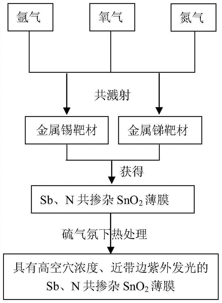
[0012] Install metal tin and metal antimony with a diameter and thickness of 60mm and 3mm respectively on the two target positions of the magnetron sputtering equipment, put the c-plane sapphire on the heating furnace (sample holder) of the growth chamber, and vacuum the system Air pressure pumped to 1×10 -4 Pa, heat the sapphire substrate to 300°C, feed a mixed gas of argon, oxygen and nitrogen with a volume ratio of 1:2:1, the gas flow rate is 40SCCM, adjust the pressure in the growth chamber to 1Pa, and place the tin target and the antimony target Adjust the sputtering power to 70W and 25W respectively, remove the two target baffles, and sputter for 60 minutes to obtain unheated Sb and N co-doped SnO 2 film. Put the film in an annealing furnace, and put 30mg of sulfur powder evenly around the film, use a vacuum pump to pump the annealing furnace pressure below 0.1Pa, and then pass in argon gas with a gas flow rate of 40 SCCM, and raise the temperature at a rate of 5°C / s A...


PUM


Abstract

The invention relates to a manufacturing method of a p-type stannic oxide thin film with the near band edge ultraviolet light emission function. The manufacturing method is characterized in that metal Sn, metal Sb, N2, O2 and powdered sulfur serve as raw materials, the p-type SnO2 thin film with the high hole concentration and the near band edge ultraviolet light emission function is manufactured through the magnetron sputtering technology and the sulfur atmosphere heat treatment technology, the hole carrier concentration range ranges from 1018 cm<-3> to 1019 cm<-3>, and the room temperature ultraviolet light emission wavelength ranges from 380 nm to 390 nm. According to the manufacturing method, the donor and acceptor element co-doping technology and the sulfur atmosphere heat treatment technology are adopted, the solid solubility of an acceptor in the SnO2 is increased, the prohibition rule of electrons on the aspects of the SnO2 bottom of conduction band and valence-band maximum transition is broken, near band edge ultraviolet light emission is achieved, and the method can be used for manufacturing a p-type conducting layer in a broad-band gap oxide photoelectric device.

Description

technical field [0001] The invention relates to a p-type SnO capable of realizing near-band-edge ultraviolet luminescence 2 The preparation method of thin film, this method uses metal tin (Sn), metal antimony (Sb), nitrogen (N 2 ), oxygen (O 2 ), argon (Ar) and sulfur powder (S) as raw materials, belonging to the field of optoelectronic thin film materials. Background technique [0002] SnO 2 It is a direct wide bandgap oxide semiconductor, its basic bandgap and optical bandgap are 3.3eV and 3.6eV respectively, because of its high visible light transmittance and strong electronic conductivity, it is used in transparent conductive films , solar cells, photocatalysis and other fields. Although SnO 2 It is a direct bandgap material, but due to the limitation of its crystal structure symmetry, the transition of electrons between the bottom of the conduction band and the top of the valence band is forbidden, that is, SnO 2 It is impossible to generate near-band-edge UV lumi...

Claims


Application Information

Patent Timeline
Patent Type & Authority Patents(China)
IPC IPC(8): C23C14/34C23C14/08C23C14/58
CPCC23C14/0036C23C14/086C23C14/5866
Inventor 李永峰贾金环姚斌丁战辉
Owner JILIN UNIV
Why Eureka
Try Eureka