A device and method for preparing copper-clad ceramic substrates by twin-target magnetron sputtering

A copper-clad ceramic substrate and target magnetron sputtering technology, used in sputtering coating, ion implantation coating, vacuum evaporation coating and other directions, can solve the problem that the adhesion between metal layer and blank ceramic sheet is difficult to meet high-power heat dissipation Substrates, metal films and blank ceramic substrates have poor adhesion and large differences in thermal expansion coefficients, so as to protect the environment, enhance adhesion and reduce costs.

Active Publication Date: 2018-04-03
SINOTENG SILICA MATERIALS TECH (JIANGSU) CO LTD
View PDF4 Cites 0 Cited by
  • Summary
  • Abstract
  • Description
  • Claims
  • Application Information

AI Technical Summary

Problems solved by technology

[0005] 1) The cost of raw materials increases due to the use of precious metals; 2) CVD usually requires high temperatures, such as 800°C~1000°C; 3) From the microstructure of the sintered blank ceramic substrate surface, there are obvious sharp protrusions and basin-shaped concave holes, while the 10 -3 ~10 -6 In the vacuum PVD process of torr, the nominal free path of atoms or molecules is quite long. Therefore, it is difficult to form a continuous and uniform film seed layer on the surface of a blank ceramic sheet. Even if the metal layer is thickened by electroplating and other methods, the metal film Poor adhesion to blank ceramic substrates; 4) Due to the large difference in intrinsic properties between metal and ceramic materials, such as a large difference in thermal expansion coefficient, the adhesion between the metal layer and the blank ceramic sheet is difficult to meet the requirements of high-power heat dissipation substrates, such as The bonding force between the metal layer and the blank ceramic substrate is greater than 500kg / cm 2 , the number of thermal cycles is higher than 50,000 times

Method used


Image

  • A device and method for preparing copper-clad ceramic substrates by twin-target magnetron sputtering
  • A device and method for preparing copper-clad ceramic substrates by twin-target magnetron sputtering
  • A device and method for preparing copper-clad ceramic substrates by twin-target magnetron sputtering

Examples


Embodiment Construction

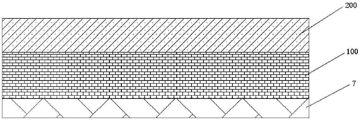
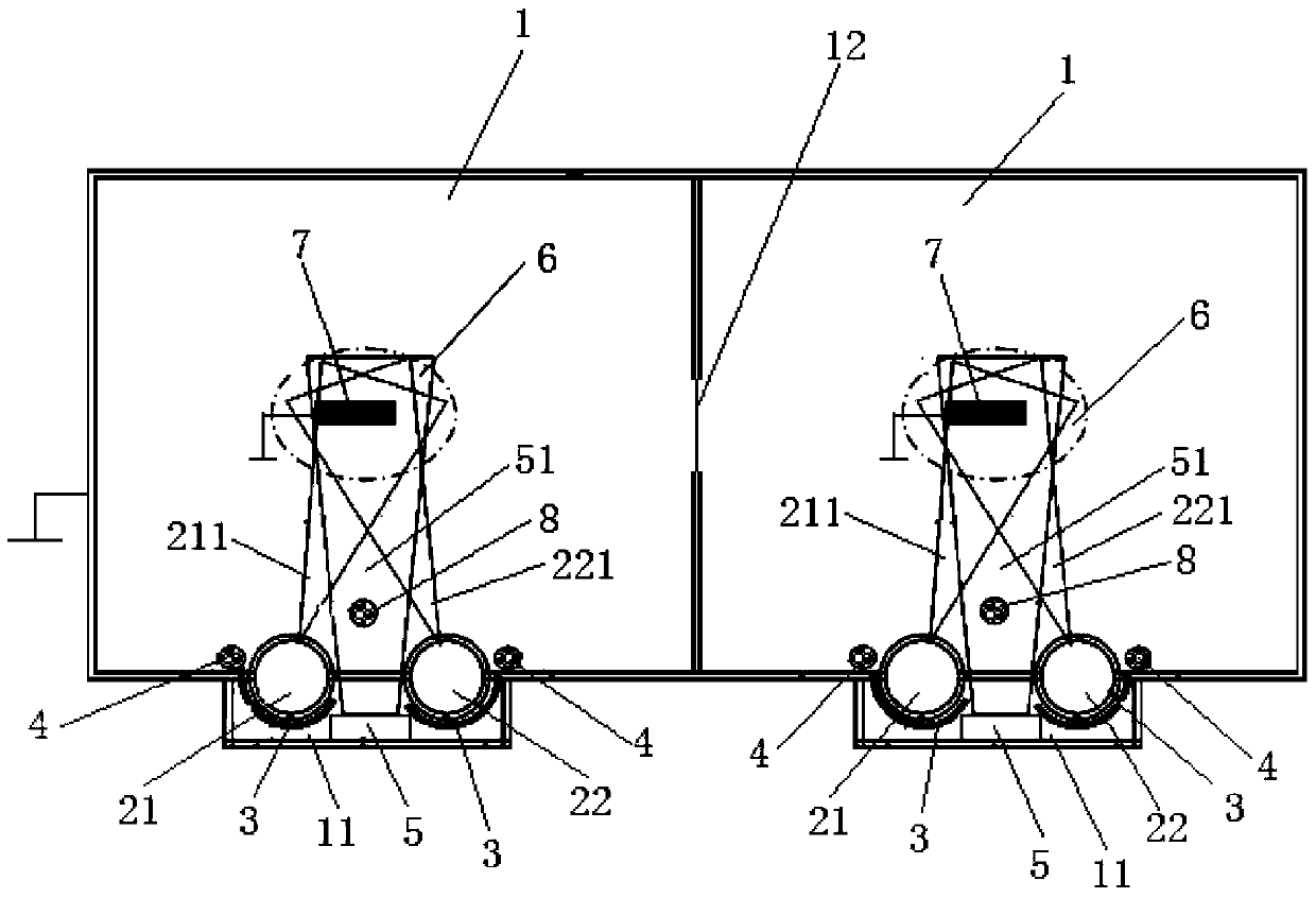
[0041] refer to Figure 1~Figure 5 , a device for preparing a copper-clad ceramic substrate by twin-target magnetron sputtering according to the present invention, comprising: at least one sputtering vacuum chamber 1, placed vertically, shaped as a cylindrical barrel or a square box, and equipped with Vacuum pump (not shown) and heating element (not shown), the inner wall of one side in the height direction protrudes outward to form a housing chamber 11; at least one pair of twin pairs of targets, each pair of twin pairs of targets corresponds to a sputtering vacuum chamber 1. It includes a metal cylindrical target 21 and a copper alloy cylindrical target 22, which are located in the sputtering vacuum chamber 1 and symmetrically arranged on both sides of the accommodating chamber 11. The metal cylindrical target 21 and the copper alloy cylindrical target 22 are yin and yang to each other Pole; at least two arc extinguishing covers 3, which are arc-shaped, and the arc is matche...


PUM

PropertyMeasurementUnit
thicknessaaaaaaaaaa

Abstract

The invention provides a device and method for preparing a copper-clad ceramic substrate by twin-target magnetron sputtering. The device includes: a sputtering vacuum chamber, one side of which forms an accommodating cavity; twin targets, including a metal cylindrical target and a copper alloy Cylindrical target; two arc extinguishers, which are rotatably arranged around the outer circumference of the metal cylindrical target and the copper alloy cylindrical target; two gas pipes, respectively located outside the metal cylindrical target and the copper alloy cylindrical target; It forms a triangular arrangement with the copper alloy cylindrical target, and the metal plasma, copper alloy plasma and argon plasma or argon and oxygen mixed plasma meet to form a plasma intersection area; an alumina ceramic substrate is erected on the plasma In the intersection area; a compensation gas pipe. The method has strong adhesion between the transition layer and the metal layer and the ceramic substrate, low raw material cost and production cost, and the preparation method protects the environment and can effectively reduce environmental pollution.

Description

technical field [0001] The invention belongs to the technical field of microelectronic packaging, and in particular relates to a device and method for preparing a copper-clad ceramic substrate by twin-target magnetron sputtering. Background technique [0002] In the field of power electronics, typical power circuit applications mainly include power semiconductor modules, DC / DC converters, optical ballasts, motor drive controllers, and automotive control systems. The rated current values ​​of various power circuits are different, and the range of variation can range from a few amperes to hundreds of amperes or even thousands of amperes, which causes the functional requirements of various power circuits to vary widely. Modern microelectronic packaging is almost always performed on or in relation to a substrate. With the emergence of new high-density packaging forms, many functions of electronic packaging, such as electrical connection, physical protection, stress relaxation, ...

Claims


Application Information

Patent Timeline
Patent Type & Authority Patents(China)
IPC IPC(8): C23C14/35C23C14/18
Inventor 何洪傅仁利何书辉齐国超
Owner SINOTENG SILICA MATERIALS TECH (JIANGSU) CO LTD
Why Eureka
Try Eureka