Dielectric material for hydrogen sensor core, hydrogen sensor core and preparation method and application thereof
A sensor core and dielectric material technology, applied in the field of sensors, can solve the problems of reducing the long-term stability and reliability of materials, low hydrogen detection sensitivity, complex preparation, etc., and achieve low raw material and preparation costs, low material and processing costs, The effect of simple preparation process
- Summary
- Abstract
- Description
- Claims
- Application Information
AI Technical Summary
Problems solved by technology
Method used
Image

Examples
Embodiment 1
[0037] A dielectric material for hydrogen sensor core body, the dielectric material is amorphous carbon.
[0038] In this embodiment, the amorphous carbon is N-doped amorphous carbon.
[0039] In this embodiment, the atomic percentage of N in the N-doped amorphous carbon is 3.68%.
Embodiment 2
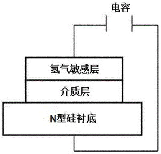
[0041] like figure 1 As shown, the hydrogen sensor core of this embodiment includes a substrate, a dielectric layer and a hydrogen sensitive layer in sequence, and the dielectric layer is an N-doped amorphous carbon film formed of the dielectric material for the hydrogen sensor core of Embodiment 1.
[0042] In this embodiment, the thickness of the N-doped amorphous carbon film is 90 nm.
[0043] In this embodiment, the substrate is a phosphorus-doped N-type silicon wafer.
[0044] In this embodiment, the resistivity of the phosphorus-doped N-type silicon substrate is 3Ω·cm˜6Ω·cm.
[0045] In this embodiment, the hydrogen-sensitive layer is a palladium-chromium alloy thin film, wherein chromium accounts for 18.3 wt%, and palladium accounts for 81.7 wt%.
[0046] In this embodiment, the thickness of the palladium-chromium alloy thin film is 30 nm.
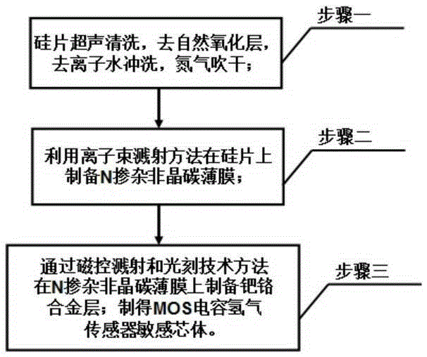
[0047] figure 2 Show the preparation method of hydrogen sensor core body of the present invention, comprise the following steps...
Embodiment 3
[0057] like figure 1 As shown, the hydrogen sensor core of this embodiment includes a substrate, a dielectric layer and a hydrogen sensitive layer in sequence, and the dielectric layer is an N-doped amorphous carbon film formed of the dielectric material for the hydrogen sensor core of Embodiment 1.
[0058] In this embodiment, the thickness of the N-doped amorphous carbon film is 90 nm.
[0059] In this embodiment, the substrate is a phosphorus-doped N-type silicon wafer.
[0060] In this embodiment, the resistivity of the phosphorus-doped N-type silicon substrate is 3Ω·cm˜6Ω·cm.
[0061] In this embodiment, the hydrogen-sensitive layer is a palladium-chromium alloy thin film, wherein chromium accounts for 18.3 wt%, and palladium accounts for 81.7 wt%.
[0062] In this embodiment, the thickness of the palladium-chromium alloy thin film is 30 nm.
[0063] The preparation method of the hydrogen sensor core body of the present embodiment comprises the following steps:
[006...
PUM
| Property | Measurement | Unit |
|---|---|---|
| Thickness | aaaaa | aaaaa |
| Resistivity | aaaaa | aaaaa |
| Resistivity | aaaaa | aaaaa |
Abstract
Description
Claims
Application Information
 - Generate Ideas
- Intellectual Property
- Life Sciences
- Materials
- Tech Scout
- Unparalleled Data Quality
- Higher Quality Content
- 60% Fewer Hallucinations
Browse by: Latest US Patents, China's latest patents, Technical Efficacy Thesaurus, Application Domain, Technology Topic, Popular Technical Reports.
© 2025 PatSnap. All rights reserved.Legal|Privacy policy|Modern Slavery Act Transparency Statement|Sitemap|About US| Contact US: help@patsnap.com