

Production technology of all-back electrode solar battery
A technology for solar cells and full back electrodes, applied in the field of solar cells, can solve the problems of increasing the resistivity of silver electrodes, complicated preparation process, damage to the PN junction of batteries, etc., and achieves simplified production process, reduced production cost, and small contact resistivity. Effect
- Summary
- Abstract
- Description
- Claims
- Application Information
AI Technical Summary
Problems solved by technology
Method used
Image

Examples
Embodiment 1
[0037] A production process for an all-back electrode solar cell, comprising the following steps:
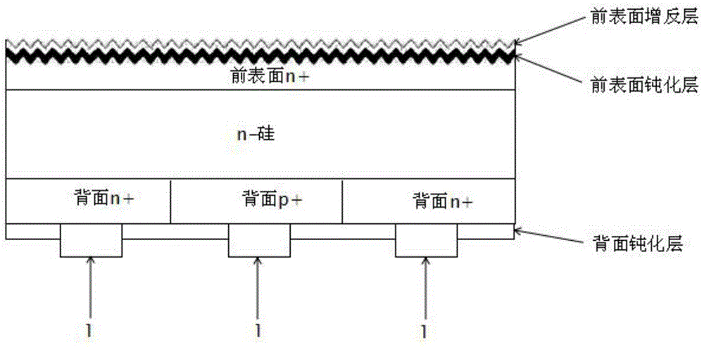
[0038] Step 1. Select n-type single crystal silicon with a resistivity of 1-12Ω·cm, with a thickness of 100-150 microns; use a diffusion furnace to perform boron diffusion on the back surface of n-type single crystal silicon to form a p+ diffusion layer area on the back; use plasma Body-enhanced chemical vapor deposition (PECVD) method deposits a mask SiNx layer on the back surface of boron diffusion; etches and removes the mask SiNx layer of the n+ type region on the back by laser etching; on the front surface of n-type single crystal silicon and Texturize the film opening area etched on the back to form a textured surface; remove the mask SiNx layer on the back; perform phosphorus diffusion on the front surface of n-type single crystal silicon to form an n+ diffusion layer on the front surface; laser etch on the back Phosphorus is diffused in the final opening area to form the...
Embodiment 2
[0053] A production process for an all-back electrode solar cell, comprising the following steps:
[0054] Step 1. Select n-type single crystal silicon with a resistivity of 3Ω·cm and a thickness of 120 microns; perform local diffusion of phosphorus and boron on the back of the n-type single crystal silicon to form a rear n+ diffusion layer area with interdigitated arrangement, The p+ diffusion layer area on the back side; phosphorus is diffused on the front surface of the n-type silicon substrate silicon wafer to form the n+ diffusion layer on the front surface;
[0055] Step 2: Perform annealing and oxidation treatment on the n-type silicon substrate silicon wafer to form an oxide layer on the front and rear surfaces of the n-type silicon substrate silicon wafer; the annealing temperature is controlled at 900 ° C, and the annealing time is controlled at 40 minutes. An oxide layer is formed on the front and rear surfaces of the silicon, and the thickness of the oxide layer is...
PUM
| Property | Measurement | Unit |
|---|---|---|
| electrical resistivity | aaaaa | aaaaa |
| thickness | aaaaa | aaaaa |
| thickness | aaaaa | aaaaa |
Abstract
Description
Claims
Application Information