Perovskite solar cell and preparation method thereof

A solar cell and perovskite technology, applied in circuits, photovoltaic power generation, electrical components, etc., can solve the problems of long electron transmission path, reduced photoelectric performance, current loss, etc., to improve photoelectric performance, reduce interface recombination, and improve optical properties effect of current

Active Publication Date: 2016-05-04
CHINA ELECTRONIC TECH GRP CORP NO 18 RES INST
View PDF3 Cites 18 Cited by
  • Summary
  • Abstract
  • Description
  • Claims
  • Application Information

AI Technical Summary

Problems solved by technology

In addition, the electron transport layer used in conventional perovskite solar cells is porous TiO 2 Thin film, more interf...

Method used


Image

  • Perovskite solar cell and preparation method thereof
  • Perovskite solar cell and preparation method thereof

Examples


preparation example Construction

[0029] The preparation method of perovskite solar cell of the present invention comprises the following steps:

[0030] (1) Etching of transparent conductive electrodes: the conductive substrate is etched and corroded by plasma to form a surface morphology with a certain roughness;

[0031] (2) Preparation of electron transport layer: cleaning the above-mentioned conductive substrate, and then preparing a seed layer by sputtering, hydrothermal method or electron beam deposition method;

[0032] The steps of preparing the seed layer by sputtering are as follows: place the processed conductive substrate into a vacuum device, and draw a vacuum to at least 8×10⁻⁴ Pa, through Ar and O 2 , the oxygen-argon flow ratio is 0.01-0.1, the working pressure is 0.5Pa, the DC magnetron sputtering current is 0.2-0.35A, and the voltage is 370-410V to obtain a dense seed layer with a thickness of 80-120nm. The dense seed layer is TiO 2 , ZnO or Al 2 o 3 electron transport layer;

[0033] T...

Embodiment 1

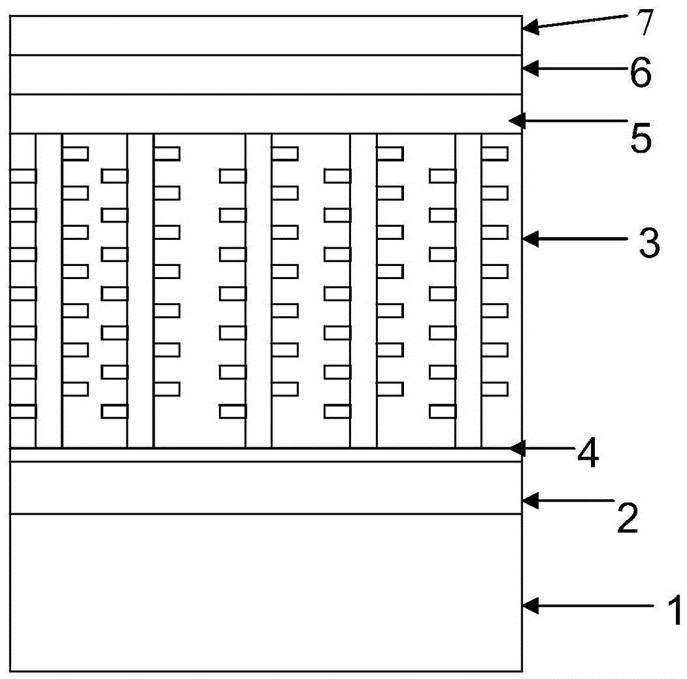
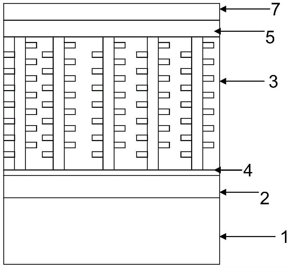
[0046] 1. Selection and treatment of substrate and upper electrode

[0047] Such as figure 1 and 2 As shown, the substrate 1 can choose flexible substrate materials such as glass, polyimide (PI), PET or PEN, and the conductive layer 2 can choose FTO (SnO 2 : F), ITO (In 2 o 3 : SnO 2 ) or IZO (In 2 o 3 : ZnO) or AZO (Al 2 o 3 : ZnO) or a mixture of several conductive materials; the conductive layer can be prepared by DC magnetron sputtering or radio frequency magnetron sputtering. Using In 2 o 3 4N purity IZO target prepared by doping 2% ZnO. Prepared by double-target DC magnetron sputtering method, the flow ratio of oxygen and argon is 0.01-0.1, the sputtering current is 0.1A-0.45A, the sputtering voltage is 300-600V, and the prepared sheet resistance is 5-10Ω / □, transparent A transparent conductive electrode with a pass rate of more than 80%. In addition, in order to increase the utilization rate of sunlight and prepare a high-quality electron transport layer 3,...


PUM

PropertyMeasurementUnit
Resistanceaaaaaaaaaa

Abstract

The invention discloses a perovskite type solar cell and a preparation method thereof. The perovskite type solar cell includes a substrate, a transparent conductive electrode, a novel electron transport layer, a perovskite layer, a hole transport layer and a metal electrode. According to the perovskite type solar cell of the invention, a hard substrate such as a glass substrate and a flexible substrate such as a polyimide (PI) or PET or PEN substrate can be selected as the substrate; and one kind of or a plurality of kinds of components selected from FTO, ITO, AZO or IZO can be adopted as the transparent conductive electrode. According to the preparation method of the perovskite type solar cell, radio-frequency direct-current magnetron sputtering or double-target direct-current magnetron sputtering can be adopted. Plasma etching or corrosion is performed on a prepared transparent conductive electrode, so that a surface form with a certain degree of roughness can be formed. The novel electron transport layer is of a nano wire (column, tube and sphere) and hybrid nano structure, which is prepared by using a hydrothermal method or an electron beam evaporation method. If the electron transport layer is applied to the perovskite type solar cell, an electron transport path can be decrease, recombination can be reduced, the utilization ratio of photo-generated carriers can be improved, and short-circuit current and the performance of the cell can be improved.

Description

technical field [0001] The invention belongs to the technical field of perovskite solar cells, and in particular relates to a novel perovskite solar cell formed by combining a nano-array novel electron transport layer with a perovskite material and a preparation method thereof. Background technique [0002] Perovskite-type methylamine-lead-iodide (halogen) thin-film solar cells (Perovskite solar cells for short) are currently a hot spot in the field of new solar cell research. From 2009 to 2015, during these six years, its photoelectric The conversion efficiency jumps from 3.8% to 20.2%, which is more than 5 times higher, and has a wide range of application prospects. [0003] Since the perovskite solar cell was proposed, it has aroused people's research enthusiasm due to the electrical, optical, magnetic and other characteristics of the perovskite material used. The most common perovskite material is lead methylamine iodide (CH 3 NH 3 PB 3 ), in terms of electricity, it...

Claims


Application Information

Patent Timeline
IPC IPC(8): H01L51/48
CPCH10K71/16H10K71/60Y02E10/549
Inventor 纪伟伟张超邓朝文乔在祥
Owner CHINA ELECTRONIC TECH GRP CORP NO 18 RES INST
Why Eureka
Try Eureka