
A kind of light-emitting diode and preparation method thereof

A technology of light-emitting diodes and insertion layers, applied in semiconductor devices, electrical components, circuits, etc., can solve the problems of weak luminous intensity and low hole concentration, and achieve the effects of reducing damage, increasing hole concentration, and reducing activation energy.

Active Publication Date: 2018-05-08
ANHUI SANAN OPTOELECTRONICS CO LTD
View PDF6 Cites 0 Cited by
  • Summary
  • Abstract
  • Description
  • Claims
  • Application Information

AI Technical Summary

Problems solved by technology

[0003] The existing P-type layer generally includes a P-type AlGaN electron blocking layer, a high-temperature P-type GaN layer and a P-type contact layer, but due to the high activation energy of magnesium in the P-type AlGaN and P-type GaN contact layers (generally P-AlGaN is 215meV , p-GaN is 175meV), only a small amount of magnesium is activated at room temperature, and the hole concentration is very low
The direct result is that most of the position of the p-n junction region falls in the p-type region, while the active light-emitting layer is doped into an n-type region due to barrier layer doping, and only a small amount of quantum wells are located in the p-n junction region to participate in the light emission, so the luminous intensity is relatively low. weak

Method used


Image

  • A kind of light-emitting diode and preparation method thereof
  • A kind of light-emitting diode and preparation method thereof
  • A kind of light-emitting diode and preparation method thereof

Examples


Embodiment 1

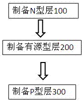
[0035] See attached figure 1 , a light-emitting diode provided by the present invention at least includes an N-type layer 100, an active layer 200, and a P-type layer 300 stacked in sequence, wherein the P-type layer 300 includes a P-type electron blocking layer 310 stacked in sequence, a high-temperature P- GaN layer 320 and P-type contact layer 330 . The N-type impurity is any one of silicon, germanium, and tin, and is used to provide electrons; the P-type impurity is any one of beryllium, magnesium, calcium, strontium, and barium, and is used to provide holes. The P-type electron blocking layer 310 is a P-type AlGaN material, and the active layer 200 is a periodic structure composed of InGaN well layers and GaN barrier layers, and the number of periods is 4-12. Since the mobility of electrons is 10 times higher than that of holes (electron mobility>1500cm 2 / vs, void 2 / vs), therefore, in order to reduce the mobility of electrons, the Al composition in the P-type electron...

Embodiment 2

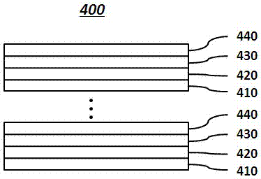
[0046] See attached Figure 5 , the difference between the present invention and Embodiment 1 is that growing a material of Al between the P-type insertion layer 400 and the P-type layer 300 x In y Ga 1-x-y The step of the transition layer 500 of N, in order to reduce the polarization effect caused by the lattice mismatch between the P-type insertion layer 400 and the P-type electron blocking layer 310, its growth temperature is between the P-type insertion layer 400 and the P-type electron blocking layer. Between the barrier layers 310, it plays a role of temperature transition, and the transition layer is Al x In y Ga 1-x-y N material layer, 0≤x<1, 0≤y<1, 0≤x+y<1. And the growth temperature of the indium source enriched layer 410, the first indium nitride layer 420, the magnesium enriched layer 430 and the second indium nitride layer 440 in the P-type insertion layer 400 is the same, and the first indium nitride layer 420 The growth time of the second indium nitride la...


PUM

PropertyMeasurementUnit
temperatureaaaaaaaaaa

Abstract

The invention belongs to the technical field of semiconductors and particularly relates to a light-emitting diode and a preparation method thereof. First an indium enrichment layer is formed on the surface of an active layer so as to be favorable for deposition of follow-up indium nitride; a magnesium Delta-doped P type insertion layer is formed through substep and low-temperature growth, and the P type insertion layer comprises the indium enrichment layer, a first indium nitride layer, a magnesium enrichment layer and a second indium nitride layer; since the energy gap of an indium nitride material is low, a magnesium source is diffused by means of an instant high magnesium concentration to enter the first indium nitride layer and the second indium nitride layer, the magnesium doping efficiency of the P type insertion layer is improved, the hole concentration of magnesium is improved, activation energy of magnesium is lowered, the position of a p-n junction region is regulated, and the internal quantum light-emitting efficiency of a device is improved. The low-temperature growing indium nitride layers can reduce damage to the active layer.

Description

technical field [0001] The invention belongs to the technical field of semiconductors, and in particular relates to a light emitting diode and a preparation method thereof. Background technique [0002] Light-emitting diode (Light-emitting diode, LED) is a kind of injection electroluminescent device, which has attracted extensive attention and application in energy saving and intelligent control. In particular, GaN-based LEDs have become the mainstream direction of LED development because their wavelengths cover the entire visible and ultraviolet bands. Therefore, how to improve the injection efficiency of carriers and thus improve the luminous performance of LEDs is a research hotspot for those skilled in the art. [0003] The existing P-type layer generally includes a P-type AlGaN electron blocking layer, a high-temperature P-type GaN layer and a P-type contact layer, but due to the high activation energy of magnesium in the P-type AlGaN and P-type GaN contact layers (gen...

Claims


Application Information

Patent Timeline
Patent Type & Authority Patents(China)
IPC IPC(8): H01L33/14H01L33/00H01L33/32
CPCH01L33/0075H01L33/14H01L33/32
Inventor 黄文宾蔡吉明黄静林兓兓张家宏
Owner ANHUI SANAN OPTOELECTRONICS CO LTD
Learn More