SERS microfluidic chip integrated with reinforced substrate on ito conductive glass and preparation method
A technology of microfluidic chips and conductive glass, applied in chemical instruments and methods, laboratory containers, material excitation analysis, etc., to achieve high sensitivity, good structure controllability and uniformity, and good signal reproducibility Effect
- Summary
- Abstract
- Description
- Claims
- Application Information
AI Technical Summary
Problems solved by technology
Method used
Image
Examples
Embodiment 1
[0033] This embodiment is the design of a microfluidic SERS chip, and the specific steps are as follows:
[0034] (1) The chip in this example consists of an ITO substrate integrated with a metal nano-SERS substrate and a PDMS cover sheet with multiple parallel channels.
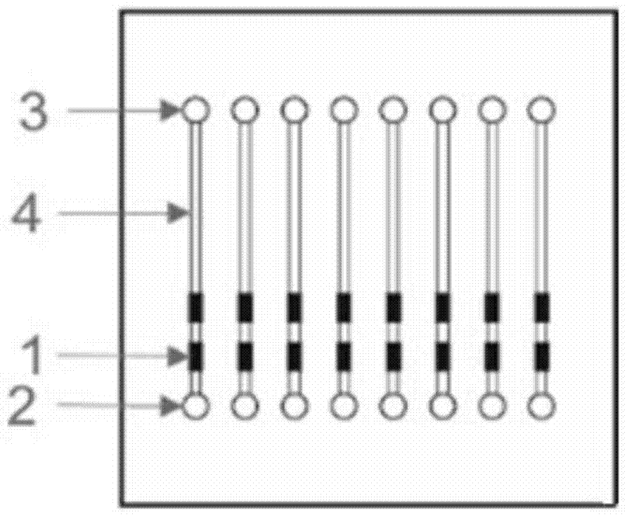
[0035] SERS chip configuration design: In this embodiment, 8 straight channels are designed on a chip of 20 × 20mm, see figure 1 , where 1 is the SERS detection area, and two SERS detection areas are set on each channel, the length of the detection area is 1mm, and the center point is 3mm and 5mm from the exit respectively. 2 and 3 are the positions of the liquid inlet and the liquid outlet, 4 is the microchannel, the length of the microchannel is 12 mm, the width is 200 μm, and the height is 150 μm.
Embodiment 2
[0036]Example 2 This example is the preparation of a PDMS cover sheet, and the specific steps are as follows: (1) Preparation of SU-8 positive film: According to the set chip configuration, on a silicon wafer, spin-coat SU-8 photoresist, Prepare the chip positive template by UV-soft lithography. The straight channel of the channel protrusion on the template is 12 mm long, 150 μm high, and 200 μm wide.
[0037] (2) Preparation of PDMS cover slip: The cover slip material selected in this example is PDMS, put the SU-8 photoresist film plate into a groove, and pour the prepolymer and the solvent according to the ratio of 1:1. The polydimethylsiloxane (PDMS) elastomer material was vacuum degassed and then placed in an oven at 90°C for 1 hour to heat and cure for 1 hour. The cured PDMS with a microchannel structure and the positive mold were uncovered and separated to obtain the following: Figure 4 b shows a PDMS cover slip with 8 microchannels. The thickness of the cover slip is...
Embodiment 3
[0040] This embodiment is to prepare an ITO conductive glass substrate integrated with a SERS active substrate, comprising the following steps:
[0041] (1) Cleaning of ITO conductive glass: Take a 20mm×20mm ITO conductive glass (resistance less than 10Ω) and use toluene, acetone, ethanol, and ultrapure water to clean it ultrasonically for 15 minutes in order to remove the oil on its surface. Dry and set aside.
[0042] (2) Electrodeposition integrated nano-silver reinforcement substrate in the SERS detection area: use electrochemical deposition technology to prepare nano-silver SERS substrate on the conductive area of the ITO conductive glass surface, the preparation process is shown in figure 2 .
[0043] First, the three-electrode system of VersaSTAT3 electrochemical workstation was adopted, with platinum electrode as counter electrode, saturated mercury aglycone electrode as auxiliary electrode, and 20mm×20mm ITO conductive glass (10Ωcm-2)) as working electrode. With ...
PUM
| Property | Measurement | Unit |
|---|---|---|
| diameter | aaaaa | aaaaa |
| width | aaaaa | aaaaa |
| depth | aaaaa | aaaaa |
Abstract
Description
Claims
Application Information


