Thin-film solar cell module and preparation method thereof

A technology of solar cells and components, applied in electrical components, circuits, photovoltaic power generation, etc., can solve problems such as high film resistance, alkali metal diffusion, resistance increase, etc., to reduce series resistance, avoid performance deterioration, and improve performance Effect

Active Publication Date: 2016-07-20
厦门神科太阳能有限公司
View PDF4 Cites 10 Cited by
  • Summary
  • Abstract
  • Description
  • Claims
  • Application Information

AI Technical Summary

Problems solved by technology

[0004] The situation is different when the transparent conductive layer covers the sidewall and bottom of the P2 trench. Due to the deposition effect of the film layer, the thickness of the transparent conductive layer deposited on the sidewall of the P2 trench is relatively thin, which causes the area The resistance of the film layer is high, which will increase the series resistance of the thin film solar cell module, thereby affecting the performance of the thin film solar cell module
[0005] Furthermore, on the sidewall of the P2 groove, the material of the transparent conductive layer is directly in contact with the material of the light absorbing layer of CuInGaSe; at the bottom of the groove of P2, the material of the transparent conductive layer is directly in contact with the material of the back electrode layer; Both the CIGS light-absorbing layer material and the back electrode layer material contain alkali metal elements. If the transparent conductive layer is in direct contact with it, the alkali metal will easily diffuse into the transparent conductive layer in this area, which will cause the The performance of the regional transparent conductive layer deteriorates (such as increased resistance, etc.), which in turn reduces the performance of thin-film solar cell modules

Method used


Image

  • Thin-film solar cell module and preparation method thereof
  • Thin-film solar cell module and preparation method thereof
  • Thin-film solar cell module and preparation method thereof

Examples


Embodiment 1

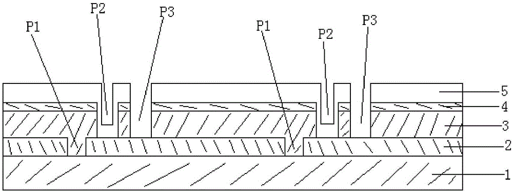
[0043] see figure 2 As shown, a kind of thin-film solar cell assembly of the present invention, when making, adopts the metal molybdenum layer of magnetron sputtering deposition 500nm on a substrate to be soda-lime glass 1 as the back electrode layer 2; Then use laser on the metal molybdenum electrode Scribe to form a P1 groove; then form copper indium gallium selenide with a chalcopyrite structure on the back electrode layer 2 as the light absorbing layer 3; deposit a 50nm CdS film layer on the light absorbing layer 3 by chemical bath (CBD) method As a buffer layer 4; then use a mechanical stylus to scribe to form a P2 trench; sputter-deposit a 15nm titanium oxide film layer on the sidewall, bottom and buffer layer 4 of the P2 trench as a high-resistance material film layer 6 , the sheet resistance of the high-resistance material film layer 6 is 350kΩ / □; adopt magnetron sputtering to deposit 800nmAZO (Al-doped ZnO) film layer on the high-resistance material film layer 6 as t...

Embodiment 2

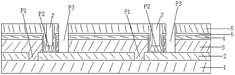
[0045] see image 3 As shown, a kind of thin-film solar cell assembly of the present invention, when making, adopts the metal molybdenum layer of magnetron sputtering deposition 500nm on a substrate to be soda-lime glass 1 as the back electrode layer 2; Then use laser on the metal molybdenum electrode Scribe to form a P1 groove; then form copper indium gallium selenide sulfur with a chalcopyrite structure on the back electrode layer 2 as the light absorbing layer 3; use a chemical bath (CBD) method to deposit a 60nm CdS film on the light absorbing layer 3 layer as the buffer layer 4; then use a mechanical stylus to scribe to form a P2 trench; then use a mask to sputter-deposit 10 nm of silicon oxide on the sidewall, bottom and part of the buffer layer 4 of the P2 trench Film layer is as high-resistance material film layer 6, and the sheet resistance of described high-resistance material film layer 6 is 5kΩ / □; Adopt magnetron sputtering deposition 600nmGZO (Ga-doped ZnO) film l...

Embodiment 3

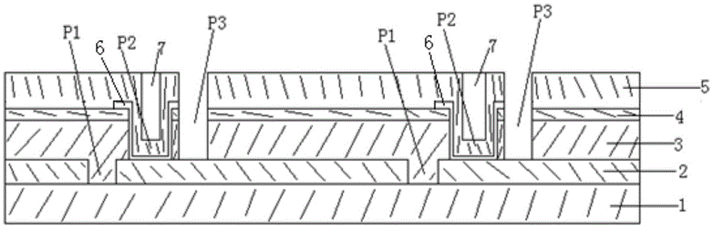
[0047] see Figure 4 As shown, a kind of thin-film solar cell assembly of the present invention, when making, adopts the metal molybdenum layer of magnetron sputtering deposition 500nm on a substrate to be soda-lime glass 1 as the back electrode layer 2; Then use laser on the metal molybdenum electrode Scribing to form a P1 groove; then forming copper indium gallium sulfide with a chalcopyrite structure on the back electrode layer 2 as the light absorbing layer 3; depositing a 40nm CdS film layer on the light absorbing layer 3 by chemical bath (CBD) method As a buffer layer 4; then use a mechanical stylus to scribe to form a P2 trench; then use a mask to sputter-deposit a 20nm aluminum-doped zinc oxide film layer on the side walls of the P2 trench and the buffer layer 4 As the high-resistance material film layer 6, the sheet resistance of the high-resistance material film layer 6 is 100kΩ / □; on the high-resistance material film layer 6, 800nm ​​BZO (B-doped ZnO) film layer is ...


PUM

PropertyMeasurementUnit
Sheet resistanceaaaaaaaaaa
Thicknessaaaaaaaaaa
Sheet resistanceaaaaaaaaaa

Abstract

The invention provides a thin-film solar cell module and a preparation method thereof. The thin-film solar cell module comprises a substrate, a back electrode layer, a semiconductor layer, a transparent conductive layer and grooves P1, P2 and P3, wherein the groove P1 is filled with a semiconductor layer material; the side walls and the bottom part of the groove P2 are covered with a high-resistance material film layer; the groove P2 is filled with a conductive material; the high-resistance material film layer is located between the side walls and / or the bottom part of the groove P2 and the transparent conductive layer; the upper part and / or the lower part of the transparent conductive layer are filled with the conductive material; the conductive material is prepared from resin or ink containing conductive particles; and the conductive particles comprise silver, aluminum, titanium, copper, molybdenum, carbon or alloys thereof and the like. The performance of the thin-film solar cell module can be improved.

Description

technical field [0001] The invention relates to the technical field of thin-film solar cells, in particular to a CIGS-based thin-film solar cell component and a preparation method thereof. Background technique [0002] With the global warming, the deterioration of the ecological environment and the shortage of conventional energy, more and more countries have begun to vigorously develop solar energy utilization technology. Solar photovoltaic power generation is a zero-emission clean energy, which has the advantages of safety, reliability, no noise, no pollution, inexhaustible resources, short construction period, and long service life, so it has attracted much attention. Copper indium gallium selenide (CIGS) is a P-type semiconductor material with a direct band gap, and its absorption coefficient is as high as 105 / cm, and a 2um thick copper indium gallium selenide film can absorb more than 90% of sunlight. The band gap of the CIGS thin film is continuously adjustable from 1...

Claims


Application Information

Patent Timeline
IPC IPC(8): H01L31/032H01L31/18H01L31/0236
CPCH01L31/0236H01L31/02363H01L31/0322H01L31/1876Y02E10/541Y02P70/50
Inventor 李艺明邓国云
Owner 厦门神科太阳能有限公司
Why Eureka
Try Eureka