Metal oxide semiconductor diode with accumulation layer

A technology of oxide semiconductor and accumulation layer, applied in semiconductor devices, electrical components, circuits, etc., can solve the problems of low forward voltage drop and high forward voltage drop, and achieve low forward voltage drop and low conduction The effect of voltage and high withstand voltage

Inactive Publication Date: 2016-07-27
UNIV OF ELECTRONICS SCI & TECH OF CHINA
View PDF3 Cites 8 Cited by
  • Summary
  • Abstract
  • Description
  • Claims
  • Application Information

AI Technical Summary

Problems solved by technology

[0004] The purpose of the present invention is to solve the problem of high forward conduction voltage drop of shallow groove metal oxide diodes in the medium and high voltage field, so that the device can achieve low forward conduction voltage drop while ensuring a high reverse withstand voltage

Method used


Image

  • Metal oxide semiconductor diode with accumulation layer
  • Metal oxide semiconductor diode with accumulation layer
  • Metal oxide semiconductor diode with accumulation layer

Examples


Embodiment 1

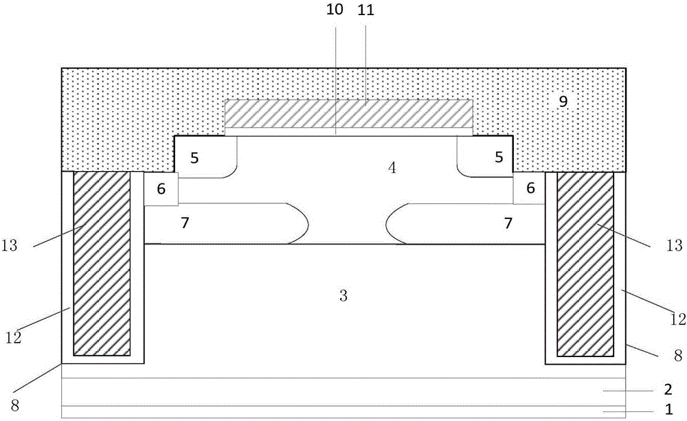
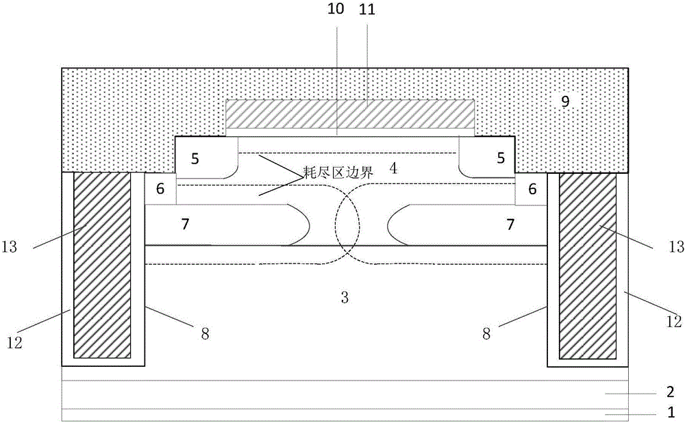
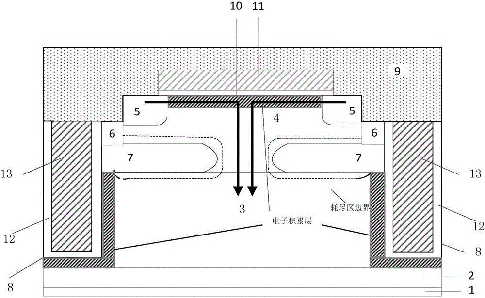
[0019] Such as figure 1 As shown, the metal oxide semiconductor diode of this example includes an anode electrode 9, an N-doped region 4, an N-type region 3, an N-type heavily doped single crystal silicon substrate 2, and a cathode stacked sequentially from top to bottom. Electrode 1; both ends of the anode electrode 9 extend vertically downward into the N-doped region 4, and there is an N-type heavily doped region 5 between the N-doped region 4 and the downwardly extending part of the anode electrode 9; The upper surface of the N-doped region 4 between the N-type heavily doped regions 5 on both sides has a planar gate structure, and the planar gate structure is located in the anode electrode 1, and the planar gate structure includes a gate oxide layer 10 and is located in the oxide The polysilicon gate electrode 11 on the upper surface of the layer 10, the lower surface of the oxide layer 10 is in contact with the upper surface of a part of the N-type heavily doped region 5; ...

Embodiment 2

[0032] Such as Figure 6 As shown, the structure of this example is based on Example 1, but the shape of the polysilicon 13 is changed. The shape of the polysilicon 13 is wide at the top and narrow at the bottom, which is an inverted trapezoid, and the oxide layer at the bottom of the groove 8 is thicker than that of the embodiment 1. The working principle of this example is similar to that of Example 1, which can further prevent the breakdown at the bottom corner of the slot 8 and increase the reverse blocking withstand voltage.

[0033] Taking Example 1 as an example, the structure of the present invention can be prepared by the following method, and the process steps are:

[0034] 1. Monocrystalline silicon preparation. An N-type heavily doped single crystal silicon substrate 2 is used, and the crystal orientation is .

[0035] 2. Epitaxial growth. An N-type epitaxial layer with a certain thickness and doping concentration is grown by methods such as vapor phase epitaxy...


PUM


Abstract

The invention relates to semiconductor technologies, in particular to a metal oxide semiconductor diode with an accumulation layer.The metal oxide semiconductor diode has the advantages that the metal oxide semiconductor diode is provided with a surface electron accumulation layer structure and a junction field effect transistor structure and accordingly can have low start voltages; the in-vivo electron accumulation layer can be formed on an N-type semiconductor surface which is in contact with a groove 8 after the metal oxide semiconductor diode is forwardly conducted, and the metal oxide semiconductor diode is provided with an N-type region 3 with high doping concentration and accordingly can have low forward voltage drop; transverse electric fields are formed between the N-type region 3 and doped polycrystalline silicon 13 when the metal oxide semiconductor diode is reversely blocked, accordingly, exhaust lines are expanded towards the N-type region 3 in an in-vivo, electric fields of a drift region are distributed in a rectangular manner, and the reverse blocking voltages of the metal oxide semiconductor diode can be increased; the metal oxide semiconductor diode is novel in structure, is high in withstand voltage and low in conduction voltage.

Description

technical field [0001] The invention relates to semiconductor technology, in particular to a metal oxide semiconductor diode with an accumulation layer. Background technique [0002] Diodes are one of the most commonly used electronic components. Traditional rectifier diodes are mainly Schottky rectifiers and PN junction rectifiers. Among them, the PN junction diode can withstand a high reverse blocking voltage and has good stability, but its forward conduction voltage drop is relatively large, and its reverse recovery time is relatively long. Schottky diodes are manufactured using the principle of metal-semiconductor junctions formed by metal-semiconductor contacts, and the on-state voltage drop is low. Due to the conduction of unipolar carriers, Schottky diodes have no excess minority carrier accumulation during forward conduction, and the reverse recovery is relatively fast. However, the reverse breakdown voltage of the Schottky diode is low, the reverse leakage current...

Claims


Application Information

Patent Timeline
Patent Type & Authority Applications(China)
IPC IPC(8): H01L29/861H01L29/06
CPCH01L29/0619H01L29/861
Inventor 任敏李爽陈哲曹晓峰李泽宏张金平高巍张波
Owner UNIV OF ELECTRONICS SCI & TECH OF CHINA
Why Eureka
Try Eureka