GaN Growth Method Based on Hexagonal Boron Nitride and Magnetron Sputtering AlN

A technology of hexagonal boron nitride and magnetron sputtering, which is applied in the field of electronics, can solve the problems of complex process, poor quality of epitaxial gallium nitride, and high background carrier concentration, so as to achieve improved material quality, excellent manufacturing performance, and good heat dissipation. The effect of stability

Active Publication Date: 2019-02-19
XIDIAN UNIV
View PDF5 Cites 0 Cited by
  • Summary
  • Abstract
  • Description
  • Claims
  • Application Information

AI Technical Summary

Problems solved by technology

However, the disadvantages of this method are: 1. Using HVPE for homoepitaxy requires metal-organic chemical vapor deposition (MOCVD) to grow gallium nitride films in advance, and the process is complicated.
2. Using hexagonal boron nitride nanosheets, the quality of epitaxial gallium nitride is poor, and the background carrier concentration is high
However, the shortcomings of this method are: 1. Graphene is easy to decompose at high temperature to produce a large amount of C impurities, and the direct growth of GaN will make the impurities diffuse into the material and affect the material quality of GaN
2. The thickness of graphene is very thin, it is difficult to effectively alleviate the lattice mismatch between the substrate and gallium nitride, which greatly limits the selection range of substrates

Method used


Image

  • GaN Growth Method Based on Hexagonal Boron Nitride and Magnetron Sputtering AlN
  • GaN Growth Method Based on Hexagonal Boron Nitride and Magnetron Sputtering AlN

Examples


Embodiment 1

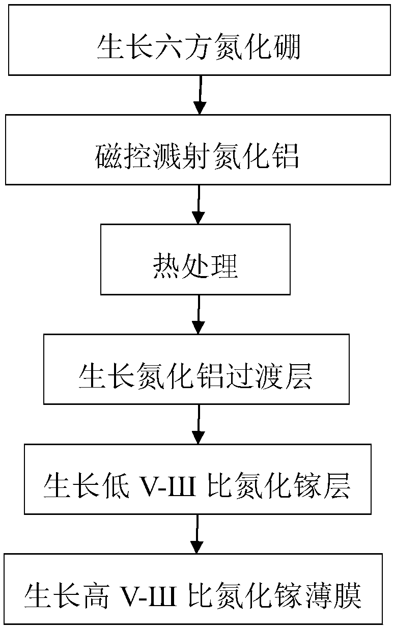
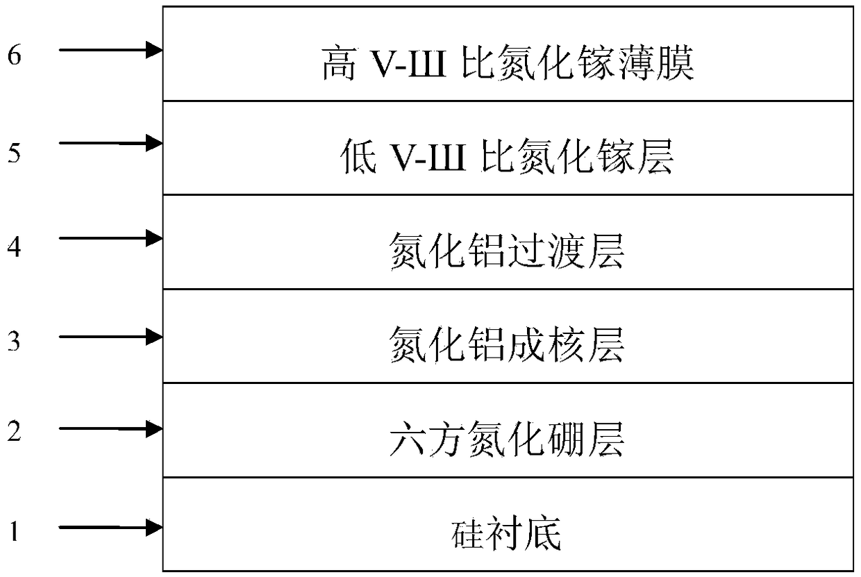
[0052] Embodiment 1: Ga-surface gallium nitride film based on hexagonal boron nitride and magnetron sputtering aluminum nitride.

[0053] Step 1. Growing a hexagonal boron nitride transition layer.

[0054] First dry the pretreated silicon substrate, put it into the microwave plasma chemical vapor deposition MPCVD reaction chamber, then evacuate the microwave plasma chemical vapor deposition MPCVD reaction chamber, and feed a small amount of hydrogen gas with a flow rate of 50 sccm. Turn on the microwave generator in the microwave plasma chemical vapor deposition MPCVD reaction chamber, start the excitation to generate plasma, and clean the silicon wafer for 10 minutes. Then feed the nitrogen gas with a purity of 99.9% and a flow rate of 150 sccm, the helium gas with a purity of 99.9% and a flow rate of 150 sccm, and the boron fluoride gas with a flow rate of 50 sccm. The boron fluoride gas is composed of 90% nitrogen and 10% boron fluoride . After raising the working pressu...

Embodiment 2

[0066] Embodiment 2: N-face gallium nitride film based on hexagonal boron nitride and magnetron sputtering aluminum nitride.

[0067] Step A. Growing a hexagonal boron nitride transition layer.

[0068] First dry the pretreated silicon wafer substrate, put it into the microwave plasma chemical vapor deposition MPCVD reaction chamber, then vacuum the microwave plasma chemical vapor deposition MPCVD reaction chamber, and feed a small amount of hydrogen gas, the flow rate of hydrogen gas is 50sccm . Turn on the microwave generator in the microwave plasma chemical vapor deposition MPCVD reaction chamber, start the excitation to generate plasma, and clean the silicon wafer for 10 minutes. Then feed the nitrogen gas with a purity of 99.9% and a flow rate of 150 sccm, the helium gas with a purity of 99.9% and a flow rate of 150 sccm, and the boron fluoride gas with a flow rate of 50 sccm. The boron fluoride gas is composed of 90% nitrogen and 10% boron fluoride . After raising the...


PUM

PropertyMeasurementUnit
thicknessaaaaaaaaaa
thicknessaaaaaaaaaa
thicknessaaaaaaaaaa

Abstract

The invention discloses a gallium nitride growing method based on hexagonal boron nitride and magnetron-sputtered aluminum nitride. The method is mainly used for improving the quality of gallium nitride material. The method comprises the following growing steps: (1) growing of a boron nitride transition layer; (2) magnetron sputtering of an aluminum nitride transition layer; (3) heat treatment; (4) growing of an aluminum nitride buffer layer; (5) growing of a gallium nitride layer with a low V-SH ratio; and (6) growing of a gallium nitride layer with a high V-SH ratio. A gallium nitride film formed according to the method has the advantages of combining hexagonal boron nitride and magnetron-sputtered aluminum nitride, having high material quality and a large applicable substrate range and being capable of being used for manufacturing high-performance gallium nitride devices.

Description

technical field [0001] The invention belongs to the field of electronic technology, and further relates to a gallium nitride growth method based on hexagonal boron nitride and magnetron sputtering aluminum nitride in the field of microelectronic technology. The invention can be used for making gallium nitride thin films and devices thereof. Background technique [0002] The third-generation semiconductors represented by gallium nitride have the advantages of large band gap, high breakdown field strength, high thermal conductivity, corrosion resistance and radiation resistance, and are widely used in optoelectronic devices and electronic devices. One of the factors that limit the quality and price of GaN-based devices is the substrate material. Due to the differences in lattice constants and other physical properties between different materials, the lattice between the substrate material and GaN single crystal Mismatch and thermal mismatch are large, so GaN thin films obtain...

Claims


Application Information

Patent Timeline
Patent Type & Authority Patents(China)
IPC IPC(8): C23C14/06C23C14/35C23C14/54C23C16/34C23C16/44C23C16/52
CPCC23C14/06C23C14/35C23C14/54C23C16/34C23C16/44C23C16/52
Inventor 张进成庞凯陈智斌吕佳骐朱家铎许晟瑞林志宇宁静张金郝跃
Owner XIDIAN UNIV
Why Eureka
Try Eureka