Self-driving two-dimensional molybdenum(IV) telluride homotype heterojunction near infrared electric detector and preparation method thereof

A technology of homogeneous heterojunction and near-infrared light, which is applied in the direction of circuits, electrical components, semiconductor devices, etc., can solve the problems of complex manufacturing process, low detection rate, non-self-driving, etc., and achieve mature and reliable technology, easy control, high The effect of detection rate

Active Publication Date: 2016-09-07
合肥庐阳科技创新集团有限公司
View PDF8 Cites 27 Cited by
  • Summary
  • Abstract
  • Description
  • Claims
  • Application Information

AI Technical Summary

Problems solved by technology

The number of film layers obtained by the first method is uncontrollable, has great randomness and cannot be produced on a large scale; while the output of the latter two methods is not high and the production process requires a high temperature environment, the production process is complex, and the equipment used is expensive
In addition, near-infrared photodetectors prepared by the above methods generally have defects such as relatively low sensitivity, relatively slow detection speed, relatively small detection rate, and non-self-driving, which seriously restrict the wide application of two-dimensional materials in the field of photoelectric detection.

Method used


Image

  • Self-driving two-dimensional molybdenum(IV) telluride homotype heterojunction near infrared electric detector and preparation method thereof
  • Self-driving two-dimensional molybdenum(IV) telluride homotype heterojunction near infrared electric detector and preparation method thereof
  • Self-driving two-dimensional molybdenum(IV) telluride homotype heterojunction near infrared electric detector and preparation method thereof

Examples


Embodiment 1

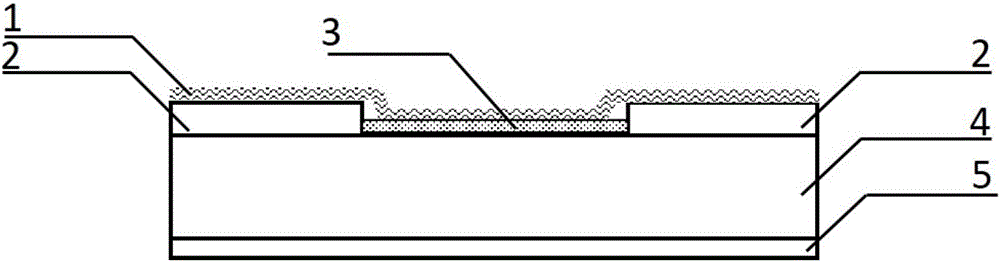
[0035] see figure 1 , the near-infrared photodetector of the present embodiment is provided with the bottom electrode 5 that is in ohmic contact with the N-type semiconductor substrate on the lower surface of the N-type semiconductor substrate 4, and the upper surface is covered with a mask layer 2; As an insulating material, a through hole is reserved in the center of the mask layer 2, and a two-dimensional molybdenum telluride thin film 3 is deposited in the through hole; the molybdenum telluride thin film is in contact with the N-type semiconductor substrate to form an N-N homogeneous heterojunction; On the upper surface of the molybdenum telluride thin film 3 is provided a top electrode 1 in ohmic contact with the N-type molybdenum telluride thin film.

[0036] Wherein, the N-type semiconductor substrate 4 of this embodiment is an N-type lightly doped silicon wafer, and the mask layer 2 is a silicon oxide layer. A lightly doped silicon wafer with a silicon oxide thickness...

experiment example 2

[0055] see figure 1 , the near-infrared photodetector of this embodiment has the same device structure as that of Embodiment 1, the only difference being that the N-type semiconductor substrate is N-type lightly doped gallium arsenide, and the mask layer is an aluminum oxide layer.

[0056] The near-infrared photodetector of the present embodiment is prepared as follows:

[0057] (1) At room temperature, N-type lightly doped gallium arsenide (with a resistance of 1-10Ω) was ultrasonically cleaned with acetone, alcohol, and deionized water for 5 minutes, and then dried with a nitrogen gun. An aluminum oxide layer with a thickness of about 200nm is evaporated on the upper surface of gallium arsenide by electron beam deposition technology as a mask layer, and a through hole with a diameter of 1 cm is left in the center of the aluminum oxide layer as a telluride molybdenum deposits;

[0058] (2) Use electron beam sputtering technology to sputter an Au electrode with a thickness ...


PUM


Abstract

The invention discloses a self-driving two-dimensional molybdenum(IV) telluride homotype heterojunction near infrared electric detector and preparation method thereof. The detector is characterized in that a bottom electrode in ohmic contact with the N type semiconductor substrate is arranged on the lower surface of an N type semiconductor substrate, the upper surface is covered by a mask layer which is made of insulating materials, a through hole is reserved in the center of the mask layer, a two-dimensional molybdenum(IV) telluride film is deposited in the through hole and is contacted with the N type semiconductor substrate to form an N-N homotype heterojunction, and the upper surface of the molybdenum(IV) telluride film is provided with a top electrode in ohmic contact with the molybdenum(IV) telluride. The near infrared electric detector is simple in preparation process, mature and reliable in technology, easy to control, and the obtained device has excellent performances of high sensitivity, high speed, high detectability, and self-driving.

Description

technical field [0001] The invention relates to a photoelectric detection semiconductor device and a preparation method thereof, in particular to a homogeneous heterojunction near-infrared photodetector based on two-dimensional molybdenum telluride. Background technique [0002] Photoelectric detection refers to a physical phenomenon in which the electrical conductivity of the irradiated material is changed by radiation. It is widely used in various fields of military and national economy, such as photoelectric communication, infrared imaging, laser guidance, etc. In recent years, with the rapid development of science and technology, two-dimensional transition metal chalcogenide detectors represented by nano-photodetection have attracted much attention due to their superior characteristics such as ultra-fast response speed, high detectivity and high sensitivity. For example, molybdenum sulfide (MoS 2 ) and silicon heterojunction have a detection rate as high as 10 under the...

Claims


Application Information

Patent Timeline
Patent Type & Authority Applications(China)
IPC IPC(8): H01L31/102H01L31/0336H01L31/18
CPCH01L31/0336H01L31/102H01L31/18Y02P70/50
Inventor 于永强许克伟耿祥顺李智罗林保
Owner 合肥庐阳科技创新集团有限公司
Why Eureka
Try Eureka