Preparation method of large-size mono-crystal perovskite film

A perovskite, large-scale technology, applied in semiconductor/solid-state device manufacturing, gaseous chemical plating, coating, etc., can solve the problems of small single crystal size, poor crystal quality, and low electrical performance of perovskite thin films. Achieve the effect of increasing size, low cost and expanding application range

Active Publication Date: 2016-09-21
海南睿德医疗器械有限公司
View PDF3 Cites 24 Cited by
  • Summary
  • Abstract
  • Description
  • Claims
  • Application Information

AI Technical Summary

Problems solved by technology

[0006] The purpose of the present invention is to solve the problem of low electrical properties caused by the small single crystal size and poor crystal quality of the perovskite film prepared in the prior art, and to provide a method for preparing a large-scale single crystal perovskite film

Method used


Image

  • Preparation method of large-size mono-crystal perovskite film
  • Preparation method of large-size mono-crystal perovskite film
  • Preparation method of large-size mono-crystal perovskite film

Examples


specific Embodiment approach 1

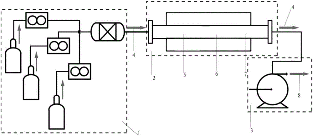
[0033] Specific embodiment one: the preparation method of the large-size single-crystal perovskite film of the present embodiment is carried out according to the following steps:

[0034] 1. Treatment of the growth substrate: the growth substrate is initially treated to obtain the processed growth substrate; the growth substrate includes mica sheet, graphite sheet, graphene, molybdenum disulfide, molybdenum diselenide, molybdenum disulfide Tungsten, tungsten diselenide, tin selenide, stannous selenide or polymer films;

[0035] The processing method of the mica sheet substrate is as follows: use adhesive tape to uncover the surface layer to expose a new surface; , the processing method of tin selenide is: need adopt chemical vapor deposition method to grow out on the silicon dioxide surface; The spin-coating instrument uses a speed of 500-10000 rpm, spin-coats for 5-90 seconds, puts the polymer film obtained by spin-coating on a heating table, and bakes it at 80-200°C for 0.5-3...

specific Embodiment approach 2

[0037] Embodiment 2: This embodiment is different from Embodiment 1 in that the polymer film is polymethyl methacrylate film, polydimethylsiloxane film or polyamide film. Other steps and parameters are the same as those in the first embodiment.

specific Embodiment approach 3

[0038] Embodiment 3: This embodiment is different from Embodiment 1 in that the organic precursor is methyl ammonium chloride, methyl ammonium iodide or methyl ammonium bromide. Other steps and parameters are the same as those in the first embodiment.


PUM

PropertyMeasurementUnit
sizeaaaaaaaaaa
sizeaaaaaaaaaa
quality scoreaaaaaaaaaa

Abstract

The invention relates to a preparation method of a large-size mono-crystal film, particularly relates to a preparation method of a large-size mono-crystal perovskite film and aims to solve a problem of low electrical performance caused by small mono-crystal size and poor crystallization quality of a perovskite film prepared through the technology in the prior art. According to the method, an organic predecessor and an inorganic predecessor are utilized, heating evaporation is realized to carry out gas phase reaction, and the large-size mono-crystal perovskite film is prepared on a substrate. Through the method, the large-size mono-crystal perovskite film with large size and high crystallization quality can be prepared, precise control on physical properties such as size, thickness and components of the film can be realized, and the large-size mono-crystal perovskite film prepared through the method can be applied to flexible solar energy cells, laser devices and LED devices.

Description

technical field [0001] The invention relates to a preparation method of a large-scale single-crystal film, in particular to a preparation method of a large-scale single-crystal perovskite film. Background technique [0002] With the development of human society, people's demand for energy is increasing day by day. At present, the world's energy is still dominated by traditional fossil energy, and the problems of resource depletion and environmental pollution caused by its use have become very prominent; whether it can find a renewable and clean energy has become a very urgent task for all countries. [0003] As a green, clean and renewable energy, solar energy is one of the important resources to solve the increasingly severe energy shortage and environmental pollution problems in the world. A solar cell refers to a type of photoelectric device that directly converts solar energy into DC power through the photoelectric effect or photochemical effect, and its core component ...

Claims


Application Information

Patent Timeline
Patent Type & Authority Applications(China)
IPC IPC(8): H01L51/48H01L51/44H01L51/42C23C16/44
CPCC23C16/44H10K71/00H10K30/87H10K30/80H10K30/00Y02E10/549H10K85/50
Inventor 张甲白学林周丽杰王振龙石琳
Owner 海南睿德医疗器械有限公司
Why Eureka
Try Eureka