Supercharge Your Innovation With Domain-Expert AI Agents!

Epitaxial wafer of light-emitting diode and growing method thereof

A technology of light-emitting diodes and growth methods, which is applied in the field of epitaxial wafers of light-emitting diodes and their growth, can solve problems such as LED luminous efficiency needs to be improved, and achieve the effect of improving luminous efficiency

Inactive Publication Date: 2016-10-26
HC SEMITEK SUZHOU
View PDF3 Cites 17 Cited by
  • Summary
  • Abstract
  • Description
  • Claims
  • Application Information

AI Technical Summary

Problems solved by technology

[0004] Existing LED epitaxial wafers alternately stack InGaN layers and GaN layers to form multiple quantum well layers to achieve recombination of electrons and holes, but the luminous efficiency of LEDs needs to be improved.

Method used


Image

  • Epitaxial wafer of light-emitting diode and growing method thereof
  • Epitaxial wafer of light-emitting diode and growing method thereof
  • Epitaxial wafer of light-emitting diode and growing method thereof

Examples


Embodiment 1

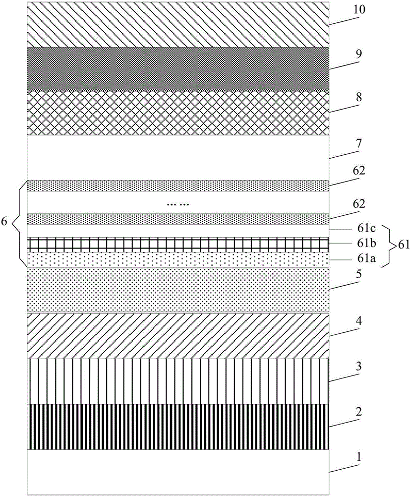
[0034] An embodiment of the present invention provides an epitaxial wafer of a light emitting diode, see figure 1 , the epitaxial wafer includes a sapphire substrate 1, and a buffer layer 2, an undoped GaN layer 3, an N-type GaN layer 4, a shallow well layer 5, a multi-quantum well layer 6, a low-temperature P Type GaN layer 7, P-type electron blocking layer 8, high-temperature P-type GaN layer 9, and P-type contact layer 10.

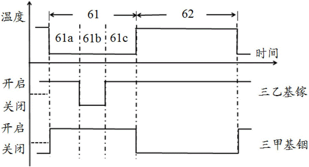
[0035] In this embodiment, the multiple quantum well layer 6 includes alternately stacked quantum well layers 61 and quantum barrier layers 62 . The quantum barrier layer 62 is a GaN layer; the quantum well layer 61 includes sequentially stacked In x Ga 1-x N layer 61a, InN layer 61b, In y Ga 1-y In the N layer 61c, 0.4z Ga 1-z N layer and GaN layer, 0<z<0.1. The P-type electron blocking layer 9 is an AlGaN layer.

[0036] Optionally, the thickness of the InN layer 61b may be 0.5-0.9 nm.

[0037] Optionally, In x Ga 1-x The thickness of the N ...

Embodiment 2

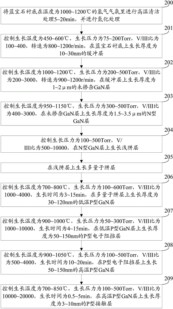
[0054] An embodiment of the present invention provides a method for growing an epitaxial wafer of a light emitting diode, which is suitable for growing the epitaxial wafer of a light emitting diode provided in Embodiment 1, see figure 2 , the growth method includes:

[0055] Step 200: Perform high-temperature cleaning treatment on the sapphire substrate in a hydrogen atmosphere at a temperature of 1000-1200° C. for 5-20 minutes, and perform nitriding treatment.

[0056] In this example, nitrogen (N 2 ) or hydrogen (H 2 ) as carrier gas, trimethylgallium (TMGa), triethylgallium (TEGa), trimethylaluminum (TMAl), trimethylindium (TMIn) and ammonia (NH3) as Ga, Al, In And N source, use silane (SiH4) and dimagnesium (CP2Mg) as N and P type dopants respectively.

[0057] Step 201: Control the growth temperature to 450-600° C., the growth pressure to 75-200 Torr, the V / III ratio to 100-400, and the rotation speed to 800-1200 r / min, and grow a buffer layer with a thickness of 10-3...

Embodiment 3

[0088] An embodiment of the present invention provides a method for growing an epitaxial wafer of a light-emitting diode. The difference between the growth method and the growth method provided in Embodiment 2 lies in that the thickness of each layer in the quantum well layer is different. Specifically, the thickness of the InN layer is 0.6-0.8nm, and the InN layer x Ga 1-x The thickness of N layer is 1~1.5nm, In y Ga 1-y The thickness of the N layer is 2-2.5 nm.


PUM

PropertyMeasurementUnit
Thicknessaaaaaaaaaa
Thicknessaaaaaaaaaa
Thicknessaaaaaaaaaa

Abstract

The invention discloses an epitaxial wafer of a light-emitting diode and a growing method thereof, and belongs to the technical field of semiconductors. The epitaxial wafer comprises a sapphire substrate, as well as a buffer layer, a GaN-undoped layer, an N-type GaN layer, a current spreading layer, a shallow well layer, a multiple quantum well layer, a low-temperature P-type GaN layer, a P-type electron blocking layer, a high-temperature P-type GaN layer and a P-type contact layer which are stacked on the sapphire substrate in sequence, wherein the multiple quantum well layer comprises quantum well layers and quantum barrier layers which are stacked alternately, each quantum barrier layer is a GaN layer, and each quantum well layer comprises an InxGa1-xN layer, an InN layer and an InyGa1-yN layer which are stacked in sequence, in which x is greater than 0.4 and smaller than 0.9, and y is greater than 0.1 and smaller than 0.5. The InN layer is inserted in the InGaN layer, so that the composition of In quantum dots is increased, more radiation recombination centers are provided, and the luminous efficiency of the light-emitting diode is improved.

Description

technical field [0001] The invention relates to the technical field of semiconductors, in particular to an epitaxial wafer of a light emitting diode and a growth method thereof. Background technique [0002] The core part of a light emitting diode (Light Emitting Diode, referred to as LED) is a wafer composed of a p-type semiconductor and an n-type semiconductor. There is a transition layer between the p-type semiconductor and the n-type semiconductor, which is called a pn junction. In the pn junction, the holes injected by the p-type semiconductor recombine with the electrons injected by the n-type semiconductor, and the excess energy is released in the form of light, which directly converts electrical energy into light energy. [0003] Group III nitrides represented by gallium nitride are wide-bandgap semiconductor materials with direct band gaps. They have high electron drift saturation speed, good thermal conductivity, strong chemical bonds, high temperature resistance, ...

Claims


Application Information

Patent Timeline
IPC IPC(8): H01L33/06H01L33/32H01L33/00
CPCH01L33/06H01L33/0066H01L33/0075H01L33/32H01L33/325
Inventor 肖云飞张华吕蒙普胡加辉
Owner HC SEMITEK SUZHOU
Features
  • R&D
  • Intellectual Property
  • Life Sciences
  • Materials
  • Tech Scout
  • Unparalleled Data Quality
  • Higher Quality Content
  • 60% Fewer Hallucinations
Learn More