Organic transistor, compound, organic semiconductor material for non-light-emitting organic semiconductor device, material for organic transistor, coating liquid for non-light-emitting organic semiconductor device, method for manufacturing organic transistor, method for manufacturing organic semiconductor film, organic semiconductor film for non-light-emitting organic semiconductor device, and method for synthesizing organic semiconductor material

A technology of organic transistors and semiconductors, applied in semiconductor/solid-state device manufacturing, semiconductor devices, chemical instruments and methods, etc., can solve problems such as evaluation of characteristics of organic transistors without mobility

Active Publication Date: 2016-11-09
FUJIFILM CORP +1
View PDF9 Cites 0 Cited by
  • Summary
  • Abstract
  • Description
  • Claims
  • Application Information

AI Technical Summary

Problems solved by technology

It should be noted that in Non-Patent Document 1, although there is a description of application to organic transistors in the preamble of Non-Patent Document 1, there is no description of the evaluation of organic transistor characteristics such as mobility.

Method used


Image

  • Organic transistor, compound, organic semiconductor material for non-light-emitting organic semiconductor device, material for organic transistor, coating liquid for non-light-emitting organic semiconductor device, method for manufacturing organic transistor, method for manufacturing organic semiconductor film, organic semiconductor film for non-light-emitting organic semiconductor device, and method for synthesizing organic semiconductor material
  • Organic transistor, compound, organic semiconductor material for non-light-emitting organic semiconductor device, material for organic transistor, coating liquid for non-light-emitting organic semiconductor device, method for manufacturing organic transistor, method for manufacturing organic semiconductor film, organic semiconductor film for non-light-emitting organic semiconductor device, and method for synthesizing organic semiconductor material
  • Organic transistor, compound, organic semiconductor material for non-light-emitting organic semiconductor device, material for organic transistor, coating liquid for non-light-emitting organic semiconductor device, method for manufacturing organic transistor, method for manufacturing organic semiconductor film, organic semiconductor film for non-light-emitting organic semiconductor device, and method for synthesizing organic semiconductor material

Examples


Embodiment 1 and comparative example 1~5

[0561]

[0562] Compound 1 of the present invention was synthesized according to the following route.

[0563] [chemical 14]

[0564] Synthesis of Intermediate 1

[0565]

[0566] [chemical 15]

[0567] Synthesis of Intermediate 2

[0568]

[0569] [chemical 16]

[0570] Synthesis of compound 1

[0571]

[0572] (Synthesis of Intermediate 1)

[0573] Add 23.1ml of tetrahydrofuran to 3.93ml of tetramethylpiperidine (TMP), stir at -78°C, add 13.8ml of n-butyllithium (1.6M hexane solution), raise the temperature to 0°C and stir for 1 hour, prepare the lithium reagent.

[0574] Add 100ml of tetrahydrofuran to 2.969g (10mmol) of thieno[3,2-f:4,5-f']bis[1]benzothiophene, stir at -78°C, and drop at -78°C using a cannula Add the above lithium reagent. The reaction liquid was cooled to -98 degreeC after 2 hours, and the solution which dissolved 9.76 g (30 mmol) of dibromodichloroethanes in 30 ml of tetrahydrofuran was dripped using the cannula. Then, the reaction solu...

Embodiment 13~24 and comparative example 6~8

[0762]

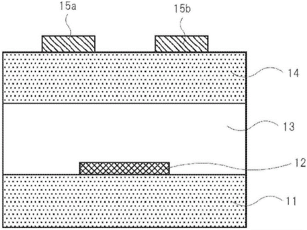
[0763] In Examples 13 to 24 and Comparative Examples 6 to 8, bottom gate-bottom contact type organic transistor devices were produced. The details are as follows.

[0764] A 0.1% by mass anisole solution of Compound 1 was heated to 100° C., and the resulting solution was cast in a nitrogen atmosphere on a substrate for measuring FET characteristics heated to 90° C. to obtain a non-luminescent organic transistor element 2 . As the substrate for measuring FET characteristics, chromium / gold (gate width W = 100 mm, gate length L = 100 μm) arranged in a comb-shaped arrangement as the source and drain, and SiO as the insulating film were used. 2 (a silicon substrate with a bottom gate-bottom contact structure with a film thickness of 200nm). The obtained device 13 was used as the organic transistor device of Example 13.

[0765] Devices 14 to 24 and Comparative Devices 6 to 8 were produced in the same manner as in Device 13 except that any one of Compounds 2 to 12 or Co...

Embodiment 25~36 and comparative example 9~11

[0771]

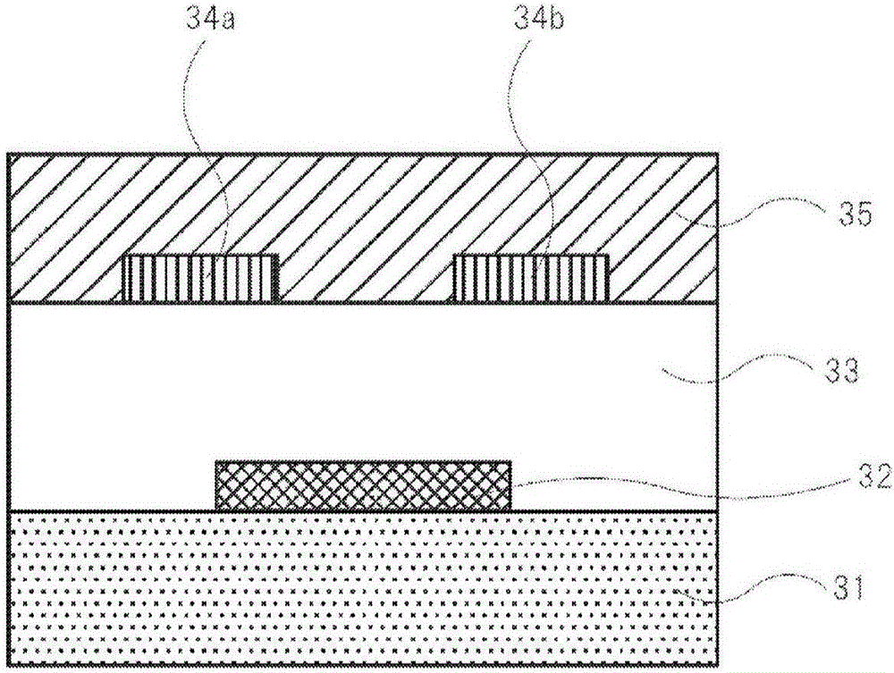
[0772] Bottom gate-bottom contact was produced in the same manner as in Example 13, except that in Example 13, a material containing Compound 1 and poly-α-methylstyrene in a mass ratio of 1:1 (Material 1') was used instead of Compound 1. type element 25. The obtained device 25 was used as the organic transistor device of Example 25.

[0773] Devices 26 to 36 and Comparative Devices 9 to 11 were produced in the same manner as in Device 25 except that any one of Compounds 2 to 12 or Comparative Compounds 1, 2, or 5 was used instead of Compound 1 in the preparation of Device 25 . The obtained elements 26 to 36 and comparative elements 9 to 11 were used as organic transistor elements of Examples 26 to 36 and Comparative Examples 9 to 11. It should be noted that materials containing compounds 2 to 12 and poly-α-methylstyrene at a mass ratio of 1:1 are referred to as materials 2' to 12', respectively.

[0774]

[0775] The FET characteristics of the organic transistor...


PUM


Abstract

The invention provides an organic transistor that has a semiconductor active layer containing a compound that can be represented by the following formula and has a molecular weight of 3,000 or less exhibits high carrier mobility (X represents an oxygen, sulfur, selenium, or tellurium atom or NR5; each Y and Z represents CR6, an oxygen, sulfur, selenium, or nitrogen atom, or NR7; the rings containing Y and Z are aromatic heterocycles; R1 or R2 may be bound to the corresponding aromatic heterocycle containing a Y and a Z via a specific divalent linking group; alternatively, R3 or R4 may be bound to the corresponding benzene ring via a specific divalent linking group; R1, R2, and R5 through R8 each represent a hydrogen atom, an alkyl group, an alkenyl group, alkynyl group, an aryl group, or a heteroaryl group; R3 and R4 each represent an alkyl group, an alkenyl group, alkynyl group, an aryl group, or a heteroaryl group; and m and n represent integers between 0 and 2, inclusive). The invention also provides a compound, an organic semiconductor material for a non-light-emitting organic semiconductor device, a material for an organic transistor, a coating liquid for a non-light-emitting organic semiconductor device, a method for manufacturing an organic transistor, a method for manufacturing an organic semiconductor film, an organic semiconductor film for a non-light-emitting organic semiconductor device, and a method for synthesizing an organic semiconductor material.

Description

technical field [0001] The present invention relates to a compound, an organic semiconductor material for a non-luminescent organic semiconductor device, a material for an organic transistor, a coating liquid for a non-luminescent organic semiconductor device, a method for producing an organic transistor, a method for producing an organic semiconductor film, and a non-luminescent organic semiconductor A method for synthesizing an organic semiconductor film and an organic semiconductor material for a device. Specifically, the present invention relates to a compound having a condensed ring skeleton structure, an organic transistor containing the compound, an organic semiconductor material for a non-luminescent organic semiconductor device containing the compound, a material for an organic transistor containing the compound, and an organic transistor containing the compound. Coating solution for non-luminescent organic semiconductor device, method for producing organic semiconduc...

Claims


Application Information

Patent Timeline
IPC IPC(8): H01L51/30C07D493/14C07D495/14C07D497/14C07D513/14C07D517/14C07D519/00H01L21/336H01L21/368H01L29/786H01L51/05H01L51/40
CPCC07D493/14C07D495/14C07D497/14C07D513/14C07D517/14C07D519/00Y02E10/549C09B57/00Y02P70/50H10K85/655H10K85/6576H10K85/657H10K10/484H10K10/466H10K71/12C09D5/24
Inventor 津山博昭野村公笃宇佐美由久福崎英治小柳雅史北村哲渡边哲也冈本敏宏竹谷纯一
Owner FUJIFILM CORP
Why Eureka
Try Eureka