High-thermostability super-junction stress Si/SiGe heterojunction bipolar transistor

A heterojunction bipolar, high thermal stability technology, used in semiconductor devices, electrical components, circuits, etc., can solve problems such as static operating point drift, aggravate thermal instability, and limit high-power stable operation of devices. Improved performance, high breakdown voltage characteristics, and effects of large current gain

Active Publication Date: 2016-11-30
BEIJING UNIV OF TECH
View PDF4 Cites 6 Cited by
  • Summary
  • Abstract
  • Description
  • Claims
  • Application Information

AI Technical Summary

Problems solved by technology

When the device is working at a high current, the self-heating effect can easily cause the drift of the static operating point and aggravate the thermal instability, which seriously limits the high-power stable operation of the device.

Method used


Image

  • High-thermostability super-junction stress Si/SiGe heterojunction bipolar transistor
  • High-thermostability super-junction stress Si/SiGe heterojunction bipolar transistor
  • High-thermostability super-junction stress Si/SiGe heterojunction bipolar transistor

Examples


Embodiment 1

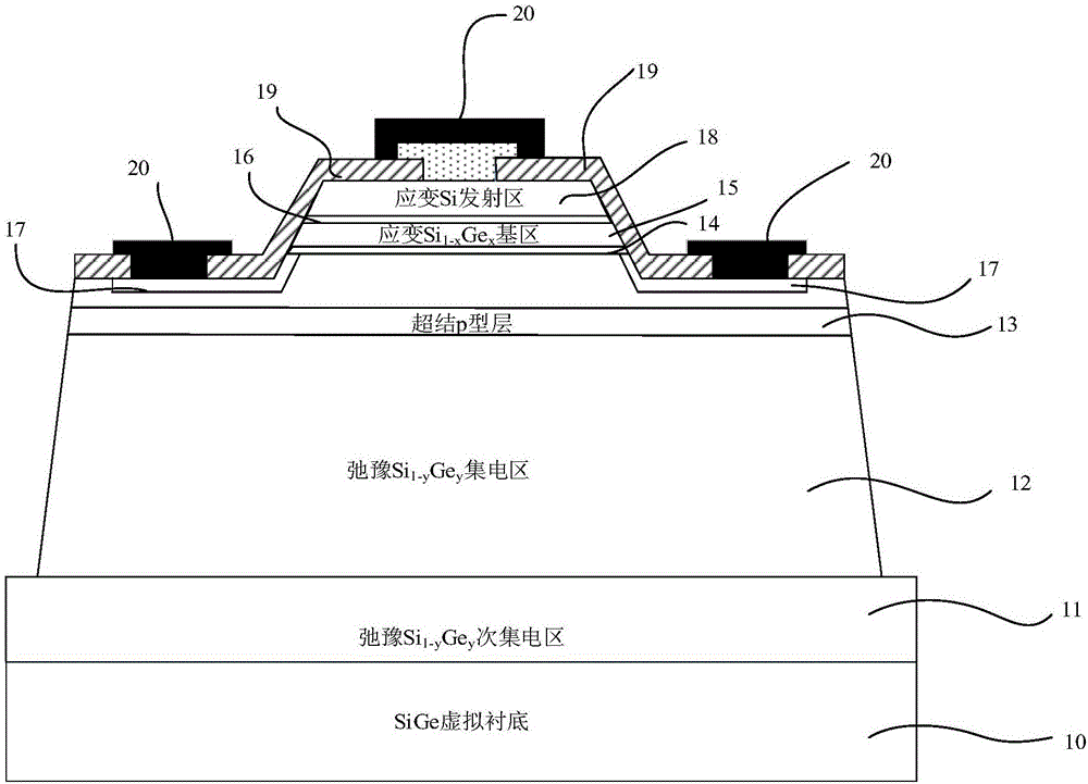
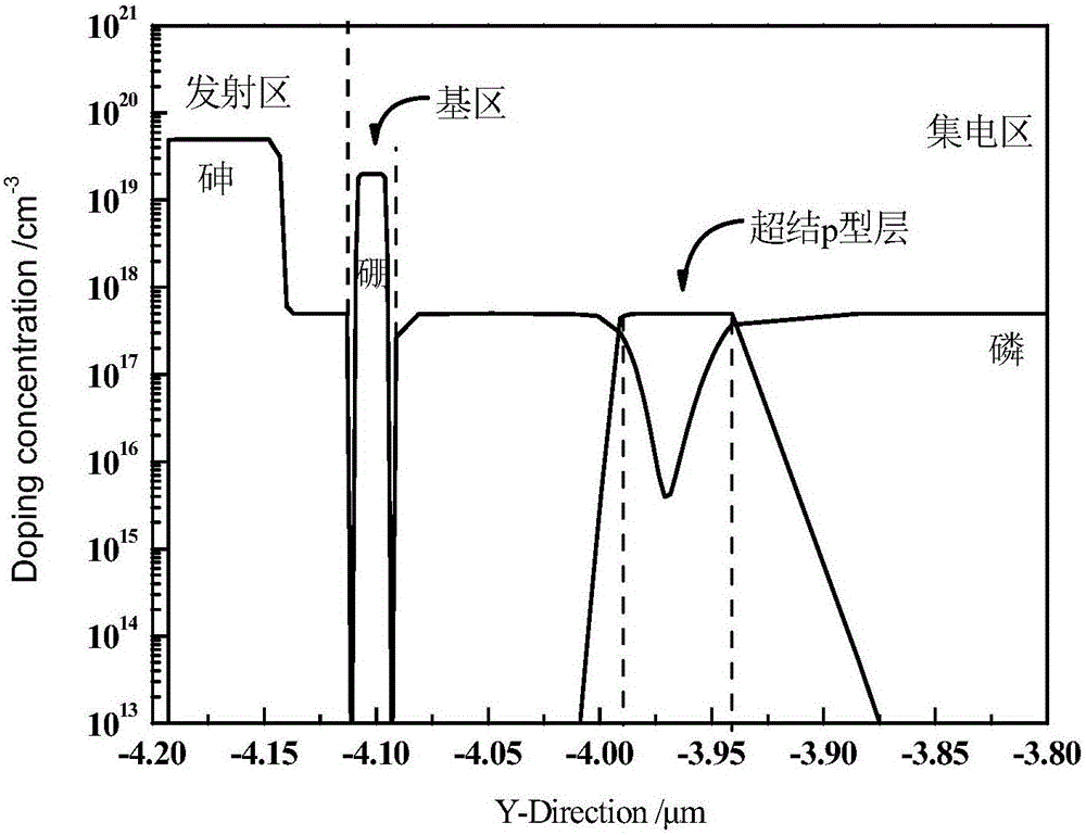
[0026] figure 1 shows the longitudinal cross-sectional structure of a strained Si / SiGe heterojunction bipolar transistor with a superjunction p-type layer, including sequentially epitaxially grown n + Doped SiGe dummy substrate (10), whose Ge content gradually changes from 0 to 0.15; n + doped relaxed Si 1-y Ge y Sub-collector (11), its Ge composition y=0.15; n - doped relaxed Si 1-y Ge y Collector region (12), its Ge composition y=0.15; superjunction p-type layer (13), intrinsically strained Si 1-x Ge x Lower buffer layer (14); p + doped strained Si 1-x Ge x Base region (15), its Ge component content x=0.3; intrinsically strained Si 1-x Ge x Upper buffer layer (16); p + Doped SiGe extrinsic base region (17); n-doped strained Si emitter region (18); silicon dioxide (SiO 2 ) layer (19) and metal leads (20).

[0027] The super junction p-type layer (13) is located on the relaxed Si 1-y Ge y In the collector region (12), parallel to the strained Si 1-x Ge x The ...

Embodiment 2

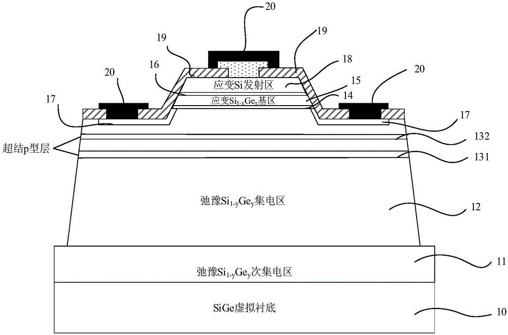
[0032] image 3 shows the longitudinal cross-sectional structure of a strained Si / SiGe heterojunction bipolar transistor with two superjunction p-type layers, including sequentially epitaxially grown n + Doped SiGe dummy substrate (10), whose Ge content gradually changes from 0 to 0.15; n + doped relaxed Si 1-y Ge y Sub-collector (11), its Ge composition y=0.15; n - doped relaxed Si 1-y Ge y Collector region (12), its Ge composition y=0.15; the lower layer of the two-layer superjunction p-type layer (131); the upper layer of the two-layer superjunction p-type layer (132); intrinsically strained Si 1-x Ge x Lower buffer layer (14); p + doped strained Si 1-x Ge x Base region (15), its Ge component content x=0.3; intrinsically strained Si 1-x Ge x Upper buffer layer (16); p + Doped Si 1-x Ge x Extrinsic base region (17), n-doped strained Si emitter region (18); silicon dioxide (SiO 2 ) layer (19) and metal leads (20).

[0033] The lower layer of the two-layer supe...


PUM


Abstract

The invention discloses a super-junction stress Si/SiGe heterojunction bipolar transistor with a high thermostability. A SiGe virtual substrate structure is adopted by the transistor; and a Si<1-y>Ge<y> secondary collector region, a relaxation Si<1-y>Ge<y> collector region, a stress Si<1-x>Ge<x> base region and a stress Si emitter region are respectively and epitaxially grown on the SiGe virtual substrate structure. According to the transistor, by introducing a super-junction p-type layer parallel to the stress Si<1-x>Ge<x> base region to the relaxation Si<1-y>Ge<y> collector region, the purposes of improving the electric field distribution in a collector junction space-charge region, reducing the peak electronic temperature, inhibiting the impact ionization and improving a device breakdown voltage are achieved; and meanwhile, with the introduction of the super-junction p-type layer, the doping concentration and the phonon scattering rate of the relaxation Si<1-y>Ge<y> collector region are effectively reduced, and the thermal conductivity of the relaxation Si<1-y>Ge<y> collector region is improved; the transistor has the characteristics of large current gain and high breakdown voltage; the internal temperature distribution is significantly reduced, the characteristic frequency and the temperature sensibility are improved, and the high-thermostability work can be realized in a relatively wide working temperature range.

Description

technical field [0001] The invention relates to a strained silicon heterojunction bipolar transistor, especially a high thermal stability superjunction strained Si used in radio frequency and microwave fields such as point-to-point wireless communication systems (>120GHz), satellite systems, optical fiber systems, and 4G / 5G mobile communication systems. / SiGe heterojunction bipolar transistors. Background technique [0002] Compared with the traditional SiGe heterojunction bipolar transistor (heterojunction bipolar transistor, HBT), strained Si / SiGe HBT has large current gain, high current handling capability and excellent high-frequency characteristics. Especially with the full development of strained technology in the fourth generation SiGe process, strained Si / SiGe HBT will be used in the fields of sensors, imagers, high-bandwidth analog-to-digital converters, automotive radars, and high-linearity amplifiers for terahertz applications. play an increasingly important r...

Claims


Application Information

Patent Timeline
Patent Type & Authority Applications(China)
IPC IPC(8): H01L29/737H01L29/16H01L29/165H01L29/06H01L29/08H01L29/10
CPCH01L29/0607H01L29/0817H01L29/0821H01L29/1004H01L29/16H01L29/165H01L29/737
Inventor 金冬月赵馨仪张万荣郭燕玲陈蕊王利凡
Owner BEIJING UNIV OF TECH
Why Eureka
Try Eureka