Perovskite photovoltaic battery taking CuyCrzO2 film as cavity transmission layer, and preparation method thereof
A technology of hole transport layer and photovoltaic cell, which is applied in the direction of photovoltaic power generation, semiconductor/solid-state device manufacturing, circuit, etc., to achieve the effect of reducing preparation cost, good photoelectric performance, and improving the ability to collect holes
- Summary
- Abstract
- Description
- Claims
- Application Information
AI Technical Summary
Problems solved by technology
Method used
Image
Examples
Embodiment 1
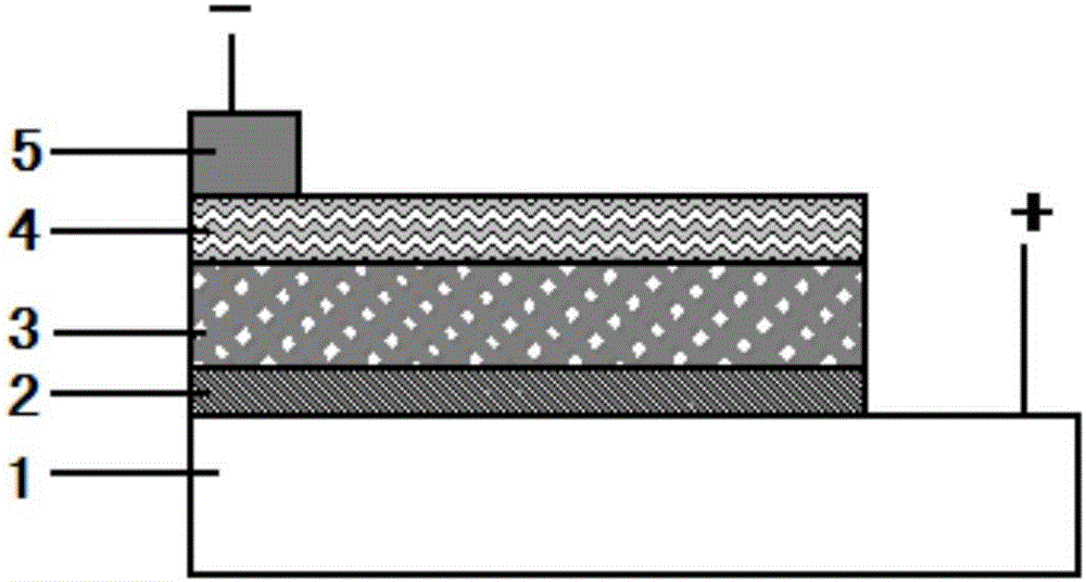
[0033] like figure 1 As shown, a Cu y Cr z o 2 A perovskite photovoltaic cell (or a planar structure perovskite photovoltaic cell) in which the thin film is a hole transport layer, including a transparent conductive substrate 1, a hole transport layer 2, a perovskite photosensitive active layer 3, and an electron transport layer 4 and a metal electrode 5, a transparent conductive substrate 1, a hole transport layer 2, a perovskite photosensitive active layer 3, an electron transport layer 4 and a metal electrode 5 are sequentially arranged in one body from bottom to top (using prior art); its preparation The method includes the following steps:
[0034] (1) Treatment of transparent conductive substrate: cleaning FTO (fluorine-doped SnO 2 ) Conductive glass slides, first put the FTO conductive glass slides into a solution containing a cleaning agent (such as Liby brand liquid detergent) and soak for 10 minutes, then repeatedly scrub and rinse with clean water; then polish w...
Embodiment 2
[0047] like figure 1 As shown, a Cu y Cr z o 2 A perovskite photovoltaic cell (or a planar structure perovskite photovoltaic cell) in which the film is a hole transport layer, including a transparent conductive substrate 1, a hole transport layer 2, a perovskite photosensitive active layer 3, and an electron transport layer 4 and a metal electrode 5, a transparent conductive substrate 1, a hole transport layer 2, a perovskite photosensitive active layer 3, an electron transport layer 4 and a metal electrode 5 are sequentially arranged into one body from bottom to top (using prior art); its preparation The method includes the following steps:
[0048] (1) cleaning ITO conductive glass sheet: cleaning method is with embodiment 1, as transparent conductive substrate 1;
[0049] (2) Prepare Cu on a transparent conductive substrate (ITO substrate) y Cr z o 2 film:
[0050] a. Dissolve 0.01 mmol of copper acetylacetonate powder with a mass purity of 99.99% and 0.01 mmol of c...
Embodiment 3
[0059] like figure 1 As shown, a Cu y Cr z o 2 A perovskite photovoltaic cell (or a planar structure perovskite photovoltaic cell) in which the thin film is a hole transport layer, including a transparent conductive substrate 1, a hole transport layer 2, a perovskite photosensitive active layer 3, and an electron transport layer 4 and a metal electrode 5, a transparent conductive substrate 1, a hole transport layer 2, a perovskite photosensitive active layer 3, an electron transport layer 4 and a metal electrode 5 are sequentially arranged in one body from bottom to top (using prior art); its preparation The method includes the following steps:
[0060] (1) cleaning of the flexible transparent plastic substrate that is coated with ITO: cleaning is the same as embodiment 1, as transparent conductive substrate 1;
[0061] (2) Prepare Cu on a transparent conductive substrate (flexible transparent plastic substrate of ITO) y Cr z o 2 film:
[0062] a. Dissolve 0.1 mmol of ...
PUM
| Property | Measurement | Unit |
|---|---|---|
| Short circuit current | aaaaa | aaaaa |
Abstract
Description
Claims
Application Information

