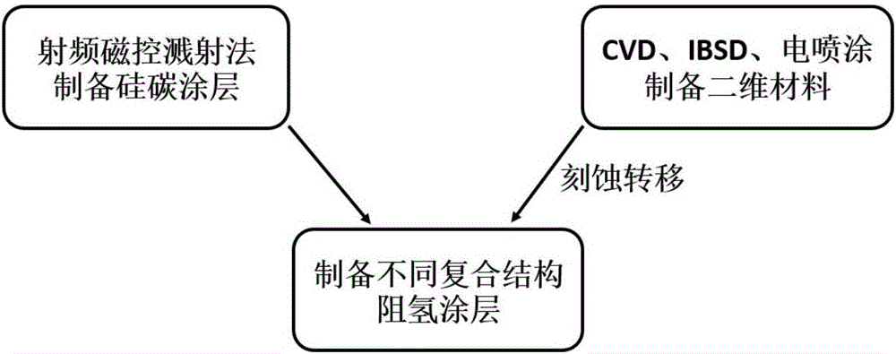
Two-dimensional material adjusting and controlling silicon-carbon composite structure hydrogen resisting coating and preparing method thereof
A two-dimensional material and two-dimensional structure technology, which is applied in the coating process of metal materials, coating, and plating of superimposed layers, etc., can solve problems such as poor hydrogen barrier performance and achieve excellent hydrogen barrier effect.
- Summary
- Abstract
- Description
- Claims
- Application Information
AI Technical Summary
Problems solved by technology
Method used
Image
Examples
Embodiment 1
[0044] 1) The 316L stainless steel substrate was mechanically polished, then ultrasonically cleaned in acetone and alcohol for 15 minutes, and dried at 80°C.
[0045] 2) Take 4 mg of graphene powder, put it into 20 ml of organic solvent NMP, and add surfactant PVP, carry out ultrasonic dissolution for 2 hours, then use a centrifuge to centrifuge at 10000r / min for 3 minutes, and take the supernatant, which is the graphene dispersion.
[0046] 3) Spray the prepared graphene dispersion on the pre-treated 316L stainless steel by electrospraying process. The process parameters are: substrate temperature 150°C, distance between nozzle and substrate 9cm, voltage 3kV, spraying rate 1mL / h, The time is 10min, after spraying in 10 -6 Under Pa vacuum, perform annealing at 400° C. for 1 h to obtain a multilayer graphene film with a thickness of about 7 nm.
[0047] 4) The silicon-carbon composite layer was prepared by radio frequency magnetron sputtering method, the inert gas Ar was used ...
Embodiment 2
[0050] 1) The 316L stainless steel substrate was mechanically polished, then ultrasonically cleaned in acetone and alcohol for 15 minutes, and dried at 80°C.
[0051] 2) The silicon-carbon composite layer was prepared by radio frequency magnetron sputtering method, the inert gas Ar was used as the sputtering gas, the target material was high-purity SiC (99.99%), and the background vacuum degree was 5×10 -4 Pa, the working pressure is 0.5Pa, deposition at room temperature, sputtering power 170W, target base distance 100mm, sputtering time 3h, on the basis of the previous step, a silicon-carbon hydrogen barrier layer was prepared with a thickness of 800nm, and then its resistance was tested. Hydrogen properties;
[0052] 3) Copper foil is used as the substrate by chemical vapor deposition, methane is used as the carbon source, and the mixed gas of hydrogen and argon is used as the carrier gas to grow graphene at 1000 ° C, and then the prepared monolayer The graphene is transfer...
Embodiment 3
[0055] 1) The 316L stainless steel substrate was mechanically polished, then ultrasonically cleaned in acetone and alcohol for 15 minutes, and dried at 80°C.
[0056] 2) The silicon-carbon composite layer was prepared by radio frequency magnetron sputtering method, the inert gas Ar was used as the sputtering gas, the target material was high-purity SiC (99.99%), and the background vacuum degree was 5×10 -4 Pa, the working pressure is 0.5Pa, room temperature deposition, the sputtering power is 200W, the target base distance is 90mm, and the sputtering time is 1h, the silicon carbon hydrogen barrier layer is prepared with a thickness of 300nm.
[0057] 3) Weigh 500mg of sulfur powder and 10mg of molybdenum trioxide and place them in a 60*30 porcelain boat, place the treated substrate on the porcelain boat with molybdenum source, and then place the two porcelain boats in two In the two temperature zones in the temperature zone chemical vapor deposition tube furnace. The inert ga...
PUM
| Property | Measurement | Unit |
|---|---|---|
| thickness | aaaaa | aaaaa |
| thickness | aaaaa | aaaaa |
| thickness | aaaaa | aaaaa |
Abstract
Description
Claims
Application Information


