Shielded gate trench power device and manufacturing method thereof

A technology of power devices and manufacturing methods, which is applied in the manufacture of shielded gate trench power devices and in the field of shielded gate trench power devices, can solve the problems of increasing gate-source leakage, reducing gate-source leakage, and reducing threshold voltage, etc., to simplify the process flow, low source-drain capacitance or gate-drain capacitance, and improved frequency characteristics

Active Publication Date: 2019-04-09
SHANGHAI HUAHONG GRACE SEMICON MFG CORP
View PDF5 Cites 0 Cited by
  • Summary
  • Abstract
  • Description
  • Claims
  • Application Information

AI Technical Summary

Problems solved by technology

[0019] It can be seen from the above that the above-mentioned polysilicon gate with sidewall polysilicon structure is a deep trench gate power device with a separated side gate structure with a shielded gate, or a shielded gate trench power device with a left and right structure, and the power device is a power MOSFET device; In the existing formation process method, the bottom-up process is used to realize the method, which is composed of Figure 1G As shown, it can be seen that the gate oxide layer 106a and the isolation dielectric layer of the shield gate, that is, the polysilicon isolation dielectric layer 106b, are formed at the same time, so that the gate oxide layer 106a determines the gap between the deep trench gate, that is, the polysilicon gate 107, and the shield gate, that is, the source polysilicon 105. When the thickness of the gate oxide layer 106a is relatively thin, it is easy to cause leakage between the gate and the source, which restricts the application of this structure in devices with low threshold voltage or turn-on voltage.
It can be seen that in order to obtain a low threshold voltage device, a thinner gate oxide layer 106a is required, and a thinner gate oxide layer 106a will simultaneously reduce the thickness of the inter-polysilicon isolation dielectric layer 106b to increase the leakage between the gate and source , so the existing method cannot solve the contradiction between lowering the threshold voltage and reducing the gate-source leakage

Method used


Image

  • Shielded gate trench power device and manufacturing method thereof
  • Shielded gate trench power device and manufacturing method thereof
  • Shielded gate trench power device and manufacturing method thereof

Examples


Embodiment Construction

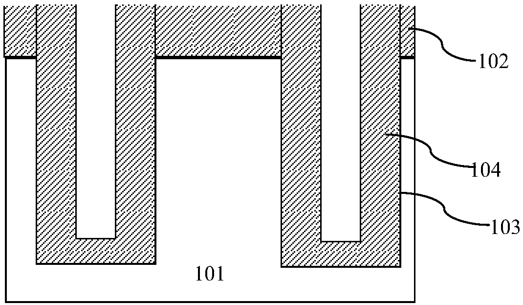
[0063] Such as figure 2 As shown, it is a schematic diagram of the structure of the shielded gate trench power device according to the embodiment of the present invention. The gate structure of the shielded gate trench power device according to the embodiment of the present invention includes:

[0064] A deep trench 201 is formed in a semiconductor substrate such as a silicon substrate 1 , and a bottom dielectric layer 2 and an isolation dielectric layer 3 between polysilicon are sequentially formed on the bottom surface and side surfaces of the deep trench 201 .

[0065] The bottom dielectric layer 2 and the inter-polysilicon isolation dielectric layer 3 do not completely fill the deep trench 201 , and the area surrounded by the inter-polysilicon isolation dielectric layer 3 forms a source trench 203 .

[0066] The bottom dielectric layer 2 at the top of the deep trench 201 is etched away by self-alignment, and a gate trench 202 is formed between the top side of the deep tre...


PUM


Abstract

The invention discloses a shield gate trench power device. A bottom dielectric layer and an inter-polysilicon isolation dielectric layer are formed in a deep trench of a gate structure, a region encircled by the inter-polysilicon isolation dielectric layer forms a source trench, a gate trench is formed in a region, on which self-alignment etching is performed, of the bottom dielectric layer arranged at a top of the deep trench, a gate dielectric layer is formed on a side surface of a top, corresponding to the deep trench, of the gate trench, a polysilicon gate is formed in the gate trench, source polysilicon is formed in the source trench, and the polysilicon gate and polysilicon of the source polysilicon are simultaneously formed. The invention also discloses a fabrication method of the shield gate trench power device. By the fabrication method of the shield gate trench power device, the threshold voltage of the device can be reduced, and meanwhile, the gate-source electric leakage of the device can be reduced; the process flow can be substantially simplified, so that the process cost is reduced; and the frequency characteristic can be improved, and the shield gate trench power device has relatively large working current density.

Description

technical field [0001] The invention relates to a method for manufacturing a semiconductor integrated circuit, in particular to a shield gate (Shield Gate Trench, SGT) trench power device; the invention also relates to a method for manufacturing a shield gate trench power device. Background technique [0002] Such as Figure 1A to Figure 1N As shown, it is a schematic diagram of the device structure in each step of the manufacturing method of the existing shielded gate trench power device; this method adopts a bottom-up method to form a deep trench separated side gate structure with a shielded gate, including the following steps : [0003] Step 1, such as Figure 1A As shown, a semiconductor substrate such as a silicon substrate 101 is provided; a hard mask layer 102 is formed on the surface of the semiconductor substrate 101, and the hard mask layer 102 can be an oxide layer, or an oxide layer plus a nitride layer. [0004] Such as Figure 1B As shown, the hard mask laye...

Claims


Application Information

Patent Timeline
Patent Type & Authority Patents(China)
IPC IPC(8): H01L29/78H01L29/423H01L21/336
CPCH01L29/4236H01L29/42364H01L29/66666H01L29/7827
Inventor 颜树范
Owner SHANGHAI HUAHONG GRACE SEMICON MFG CORP
Why Eureka
Try Eureka