Room-temperature adjustable sub-Terahertz wave detector and preparation method

A hertz wave and detector technology, applied in the field of light guide-like and photovoltaic-like detection, can solve the problems of limiting device bandwidth and speed, high noise, low sensitivity, etc., and achieve the effect of improving miniaturization, improving integration, and avoiding strong reflection

Active Publication Date: 2017-02-01
安徽荣程电子科技有限公司
View PDF6 Cites 25 Cited by
  • Summary
  • Abstract
  • Description
  • Claims
  • Application Information

AI Technical Summary

Problems solved by technology

However, such devices generally work at low temperatures, have low sensitivity and relatively large noise.
Plasma waves are excited in the channel at room temperature, the high mobility of the material is the key factor, and the distributed resistance also limits the bandwidth and speed of the device

Method used


Image

  • Room-temperature adjustable sub-Terahertz wave detector and preparation method
  • Room-temperature adjustable sub-Terahertz wave detector and preparation method
  • Room-temperature adjustable sub-Terahertz wave detector and preparation method

Examples


Embodiment 1

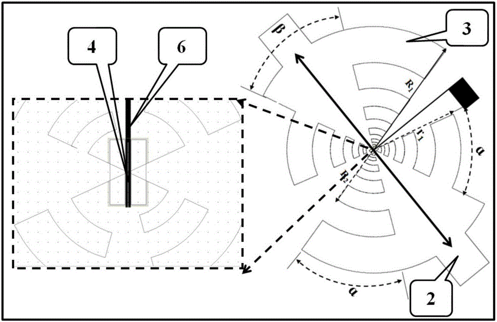
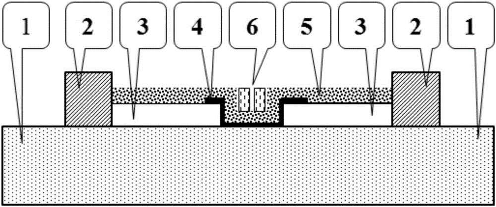
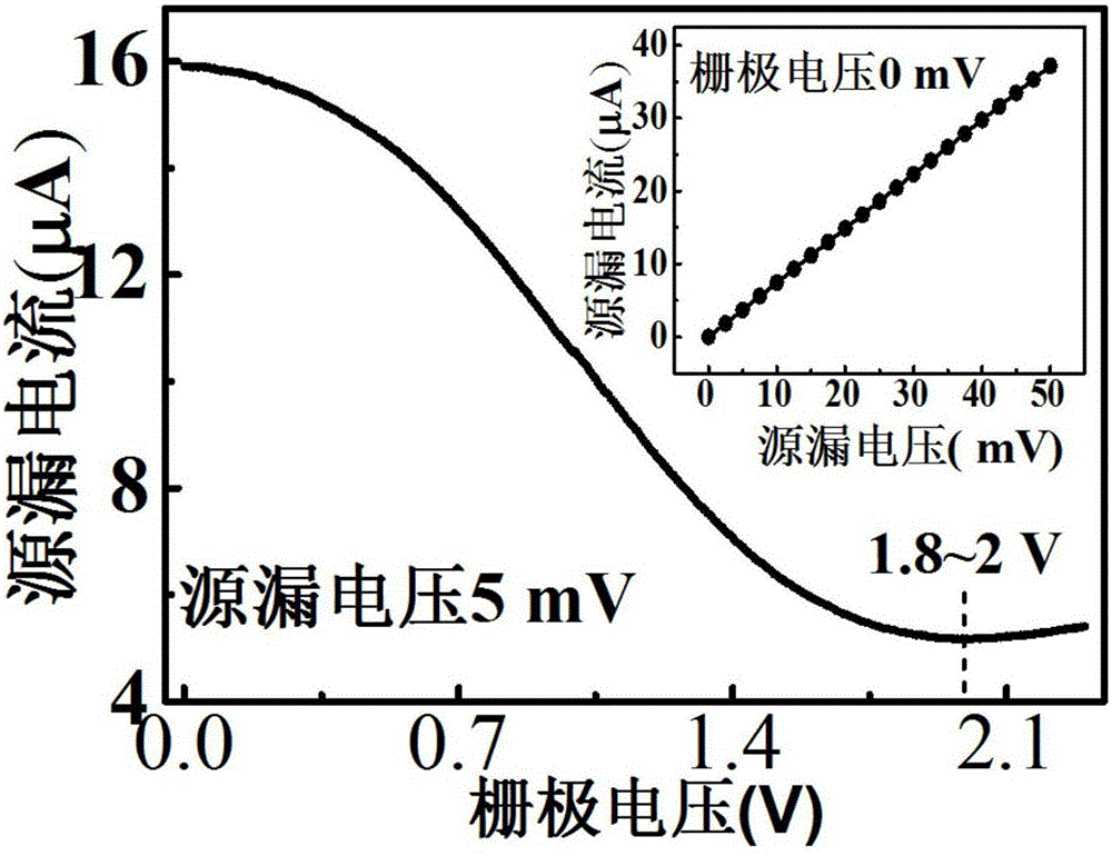
[0052] The thickness of the sapphire substrate is 1mm, when the outer radius of the logarithmic periodic antenna is 1mm, the arc is 50°, the line width of the split gate is 1μm, the line spacing is 500nm, the thickness of the aluminum oxide gate dielectric layer is 30nm, and the conductive channel CVD graphene with a length of 5μm (concentration about 10 13 cm -2 , the mobility is about 1000~5000cm 2 V -1 the s -1 ). Such as image 3 As shown, the electrical performance of the graphene field effect tube is good, and the gate control realizes the doping of graphene P and N types, and the voltage of the Dirac point is around 1.8-2V; from image 3 It can be seen from the inset that the graphene and the log-periodic antenna form a good ohmic contact, laying the foundation for the device for sub-terahertz wave detection.

Embodiment 2

[0054] The thickness of the sapphire substrate is 1mm, when the outer radius of the logarithmic periodic antenna is 2mm, the arc is 50°, the line width of the split grid is 2μm, the line spacing is 600nm, the thickness of the aluminum oxide gate dielectric layer is 50nm, and the conductive channel CVD graphene with a length of 6μm (concentration about 10 13 cm -2 , the mobility is about 1000~5000cm 2 V -1 the s -1 ),Such as Figure 4 As shown, the change of photocurrent was observed in real time under the irradiation of sub-sub-Hz wave of 0.02-0.4 THz by semiconductor analyzer. It can also be seen that the gate voltage control realizes different doping types of graphene. Compared with the dark current, the resistance of P-type doped graphene becomes larger and the photocurrent becomes smaller, while the resistance of N-type doped graphene is small and the current becomes smaller. large; and the change trend of the photocurrent amplitude of the two types of doped graphene ...

Embodiment 3

[0056] The thickness of the sapphire substrate is 0.5mm, when the outer radius of the logarithmic periodic antenna is 1mm, the arc is 50°, the line width of the split gate is 2.2μm, the line spacing is 600nm, the thickness of the aluminum oxide gate dielectric layer is 30nm, and the conductive channel CVD with a length of 10μm Graphene (concentration about 10 13 cm -2 , the mobility is about 1000~5000cm 2 V -1 the s -1 ), under zero bias voltage and sub-terahertz irradiation, the device generates photocurrent, which is similar to a photovoltaic device and has a high signal-to-noise ratio; as the bias voltage increases, it is similar to a photoconductive device, and the photoresponse also increases. It is consistent with the photoconductive type results of the detectors at both ends of the graphene antenna.

[0057] Various parameters in the detector structure change within a certain range. A room temperature-adjustable sub-terahertz wave detector in the present invention h...


PUM


Abstract

The invention discloses a room-temperature adjustable sub-Terahertz wave detector and a preparation method. A graphene field effect transistor with high migration rate and adjustable carrier concentration is taken as a basic structure unit, and the field effect transistor is provided with a group of source and drain electrodes and cleavage grid electrodes of a sub-Terahertz wave coupled antenna. The detector is integrated with log-periodic antennas and corresponding feed electrodes on a sapphire substrate; the detector is provided with a graphene conducting channel transferred in an antenna distance; an aluminum oxide gate dielectric layer is arranged on the graphene conducting channel, and finally the cleavage grid electrodes and the corresponding lead electrodes are integrated on the aluminum oxide gate dielectric layer of the graphene conducting channel, so that adjustable sub-Terahertz wave detection is realized. The detector has the advantages that the detector is an adjustable lightguide-like and photovoltaic-like detector with high speed, wide band and high response; and the integration level, technical maturity and repeatability of the device lay the foundation of large-scale application of Terahertz detectors.

Description

technical field [0001] The invention relates to a terahertz wave detector, in particular to a field effect tube pair of 0.02-0.4 split grid / alumina grid dielectric layer / graphene / logarithmic periodic antenna / sapphire substrate structure at room temperature THz sub-sub-hertz waves realize high-speed, broadband, high-response, and adjustable photoconductive and photovoltaic-like detection. Background technique [0002] Terahertz wave is the frequency of 0.1 ~ 10THz (1THz = 10 12 Hz) range, with a wavelength range of 3 mm to 30 μm, located between millimeter waves (submillimeter waves) and infrared waves. Terahertz photons correspond to an energy range of 0.414-41.4meV, which matches the low-frequency vibration and rotational energy range of molecules and materials. These determine the special position of terahertz waves in the electromagnetic spectrum and the characteristics and applications that are significantly different from millimeter waves and infrared rays in terms of...

Claims


Application Information

Patent Timeline
Patent Type & Authority Applications(China)
IPC IPC(8): H01L31/102H01L31/0224H01L31/028H01L31/18
CPCH01L31/022408H01L31/028H01L31/102H01L31/1804Y02E10/547Y02P70/50
Inventor 王林刘昌龙唐伟伟郭万龙陈效双陆卫
Owner 安徽荣程电子科技有限公司
Why Eureka
Try Eureka