Ito sputtering target and method for manufacturing same, ito transparent electroconductive film, and method for manufacturing ito transparent electroconductive film

A technology of transparent conductive film and manufacturing method, which is applied in the field of ITO sputtering target, can solve problems such as large grain size, achieve high density, guarantee improvement and reliability, and excellent reliability

Active Publication Date: 2017-02-22
JX NIPPON MINING & METALS CO LTD
View PDF16 Cites 5 Cited by
  • Summary
  • Abstract
  • Description
  • Claims
  • Application Information

AI Technical Summary

Problems solved by technology

Formula (1): the relative density (%) of the central part in the thickness direction of the sintered body / the density (%) of the entire sintered body ≥ 0.995, but the sintering temperature of the examples and comparative examples is as high as 1600 ° C, although it is not described, But it is speculated that the grain size is large
[0020] In addition, none of the above-mentioned documents considers production from the viewpoint of changing the tin oxide-rich phase by low-temperature sintering to achieve small particle size, high density, and high strength.

Method used


Image

  • Ito sputtering target and method for manufacturing same, ito transparent electroconductive film, and method for manufacturing ito transparent electroconductive film
  • Ito sputtering target and method for manufacturing same, ito transparent electroconductive film, and method for manufacturing ito transparent electroconductive film
  • Ito sputtering target and method for manufacturing same, ito transparent electroconductive film, and method for manufacturing ito transparent electroconductive film

Examples


Embodiment 1

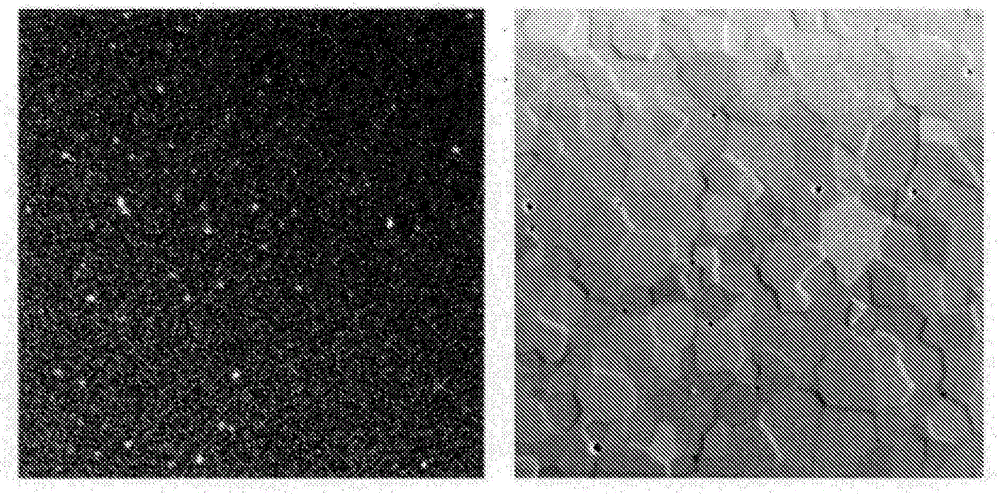
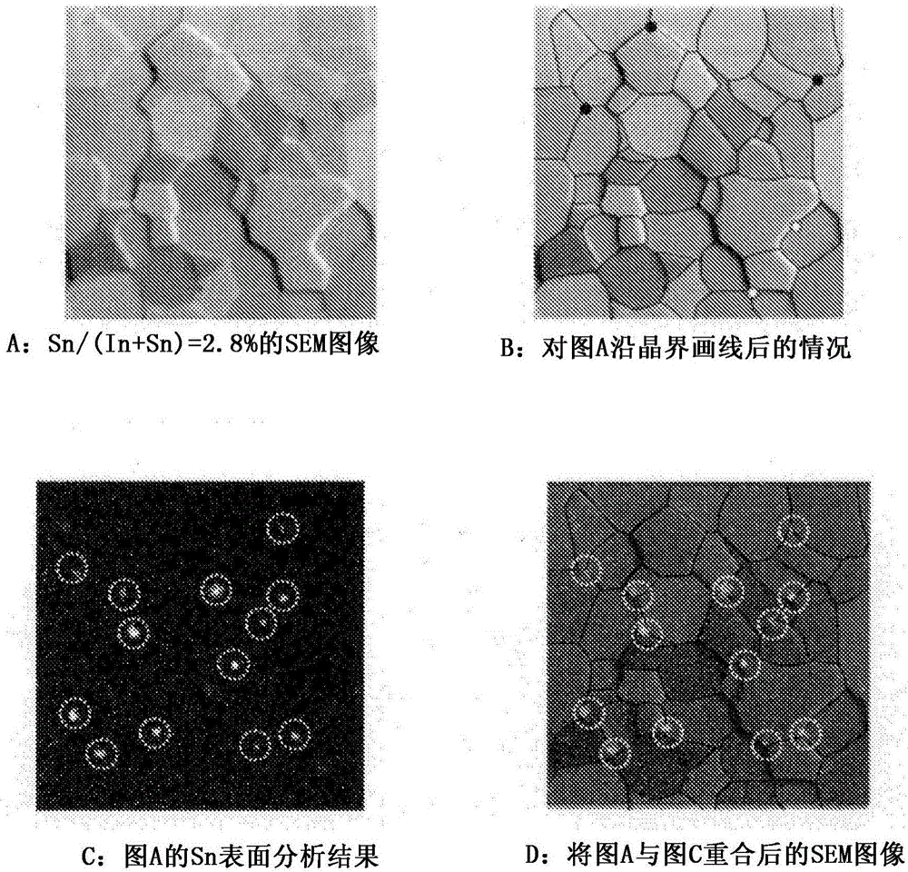
[0113] Use SnO whose ratio is adjusted so that Sn / (In+Sn) is 2.8% in atomic ratio 2 Powder and In 2 o 3 The powder was sintered in an oxygen atmosphere as a sintering raw material. The highest sintering temperature was set to 1450° C., and the holding time at the highest sintering temperature was set to 5 hours. Then, it was held at 1350° C. for 1 hour while cooling down. The sintered body obtained in this way has a sintered body density of 7.070 g / cm 3 , the bending strength is 115MPa, the volume resistivity is 0.110mΩ·cm, the average grain size is 3.43μm, the area ratio of the tin oxide-rich phase is 0.45%, the probability of the existence of the triple point of the tin oxide phase is 98%, and the pore area ratio is 0.08%.

[0114] Using this sintered body to make a target, the DC power density is 2.3W / cm 2 , The gas pressure is 0.6Pa, the sputtering gas is argon (Ar), and the gas flow rate is 300 sccm, and the sputtering is carried out continuously for 35 hours. As a ...

Embodiment 2

[0118] Use SnO whose ratio is adjusted so that Sn / (In+Sn) is 2.8% in atomic ratio 2 Powder and In 2 o 3 The powder was sintered in an oxygen atmosphere as a sintering raw material. The highest sintering temperature was set to 1450° C., and the holding time at the highest sintering temperature was set to 10 hours. Then, it was held at 1330° C. for 1 hour while cooling down. The sintered body obtained in this way has a sintered body density of 7.100 g / cm 3 , the bending strength is 120MPa, the volume resistivity is 0.116mΩ·cm, the average grain size is 3.54μm, the area ratio of the tin oxide-rich phase is 0.39%, the probability of triple point existence of the tin oxide phase is 99%, and the pore area ratio is 0.07%.

[0119] Using this sintered body to make a target, the DC power density is 2.3W / cm 2 , The gas pressure is 0.6Pa, the sputtering gas is argon (Ar), and the gas flow rate is 300sccm, and the sputtering is carried out continuously for 35 hours. As a result, the...

Embodiment 3

[0130] Use SnO whose ratio is adjusted so that Sn / (In+Sn) is 2.8% in atomic ratio 2 Powder and In 2 o 3 The powder was sintered in an oxygen atmosphere as a sintering raw material. The highest sintering temperature was set to 1450° C., and the holding time at the highest sintering temperature was set to 15 hours. Then, it was held at 1370° C. for 1 hour while cooling down. The sintered body obtained in this way has a sintered body density of 7.105 g / cm 3 , the bending strength is 121MPa, the volume resistivity is 0.124mΩ·cm, the average grain size is 3.66μm, the area ratio of the tin oxide-rich phase is 0.35%, the probability of the existence of triple points of the tin oxide phase is 99%, and the pore area ratio is 0.05%.

[0131] Using this sintered body to make a target, the DC power density is 2.3W / cm 2 , The gas pressure is 0.6Pa, the sputtering gas is argon (Ar), and the gas flow rate is 300 sccm, and the sputtering is carried out continuously for 35 hours. As a re...


PUM

PropertyMeasurementUnit
particle sizeaaaaaaaaaa
densityaaaaaaaaaa
electrical resistivityaaaaaaaaaa

Abstract

The present invention relates to a sputtering target characterized by being a sintered compact comprising In, Sn, O, and unavoidable impurities, the sintered compact containing Sn in an atomic ratio Sn / (In + Sn) of 1.8% to 3.7% (excluding 3.7%), the average crystal grain size of the sintered compact being in the range of 1.0-5.0 [mu]m, vacancies having a major-axis diameter of 0.1-1.0 [mu]m constituting an area ratio of 0.5% or less, the sintered compact having two phases including an indium oxide phase and a tin-oxide-rich phase, the area ratio of the tin-oxide-rich phase being 0.1-1.0%, and 95% or more of the tin-oxide-rich phase being present at grain boundary triple points. The present invention makes it possible to provide an ITO sputtering target suitable for forming a transparent electroconductive film and which has a low tin oxide content and enables a low-resistance film to be obtained even at low temperature, the sputtering target having a small grain size, high density, and high strength, and making it possible to reduce the occurrence of arcing or nodules.

Description

technical field [0001] The present invention relates to an ITO sputtering target suitable for forming an ITO film. In particular, it relates to an ITO sputtering target which has a small particle size, high density, and high strength, and which can reduce arc discharge or nodules, its manufacturing method, an ITO transparent conductive film, and a manufacturing method of the ITO transparent conductive film. As main applications of the present invention, touch panels, flat panel displays, organic electroluminescence (EL), and solar cells may be mentioned. Background technique [0002] In general, ITO (indium-tin composite oxide) films are widely used as transparent electrodes (conductive films) in display devices centered on liquid crystal displays. As a method of forming this ITO film, means generally called a physical vapor deposition method, such as a vacuum vapor deposition method and a sputtering method, can be used. In particular, the magnetron sputtering method is of...

Claims


Application Information

Patent Timeline
Patent Type & Authority Applications(China)
IPC IPC(8): C23C14/34C04B35/00C23C14/08H01B5/14H01B13/00
Inventor 挂野崇
Owner JX NIPPON MINING & METALS CO LTD
Why Eureka
Try Eureka