
Preparation process for double plating layers capable of inhibiting growth of lead-free solder joint interface compound, of substrate

A preparation process and a technology of lead-free solder joints, which are applied in metal material coating process, liquid chemical plating, plating of superimposed layers, etc., can solve problems that have not been reported, and achieve simple and easy operation, good effect, Even and fine plating effect

Active Publication Date: 2017-03-08
NANCHANG UNIV
View PDF6 Cites 2 Cited by
  • Summary
  • Abstract
  • Description
  • Claims
  • Application Information

AI Technical Summary

Problems solved by technology

[0006] At present, the coatings used for the barrier layer of electronic packaging are mainly concentrated on the electroless Ni-P or Ni-W-P single layer, and there is no report on the Ni-W-P / Cu double coating

Method used


Image

  • Preparation process for double plating layers capable of inhibiting growth of lead-free solder joint interface compound, of substrate
  • Preparation process for double plating layers capable of inhibiting growth of lead-free solder joint interface compound, of substrate
  • Preparation process for double plating layers capable of inhibiting growth of lead-free solder joint interface compound, of substrate

Examples


Embodiment 1

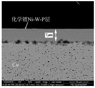
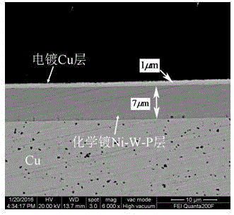
[0032] The invention discloses a double coating preparation process of electroless plating Ni-W-P / electroplating Cu on a metal substrate that inhibits the growth of lead-free solder joint interface compounds. Pure copper is selected as the metal substrate, and a layer of Ni-W-P is chemically plated on the metal substrate first, the thickness of the coating is about 3~10µm, and then a thinner layer of copper is electroplated on it, and the thickness of the electroplating layer is about 0.5~3µm.

[0033] The preparation of the electroless plating solution is to mix nickel sulfate, sodium citrate, sodium hypophosphite, lactic acid, ammonium chloride and sodium tungstate, add water and stir evenly, and then use ammonia solution to adjust the pH to 7; the nickel sulfate in the electroless plating solution is 30g / L, sodium citrate is 35g / L, sodium hypophosphite is 30g / L, lactic acid is 16ml / L, ammonium chloride is 1mol / L, and sodium tungstate is 30g / L. Drugs such as nickel sulfate,...

Embodiment 2

[0037] The method of the present embodiment is the same as Example 1, except that sodium citrate is 30g / L, and potassium pyrophosphate is 300g / L. The resulting electroless plating rate is about 2.75 µm / h and the electroplating rate is 0.19 µm / min.

Embodiment 3

[0039] The method of the present embodiment is with embodiment 1, and difference is that nickel sulfate is 35g / L, and potassium pyrophosphate is 200g / L. The resulting electroless plating rate was about 2.88 µm / h and the electroplating rate was 0.18 µm / min.


PUM

PropertyMeasurementUnit
thicknessaaaaaaaaaa
thicknessaaaaaaaaaa
thicknessaaaaaaaaaa

Abstract

The invention discloses a preparation process for double plating layers capable of inhibiting the growth of a lead-free solder joint interface compound, of a substrate. The double plating layers comprise a chemical plating Ni-W-P layer and an electroplating Cu layer. The chemical plating Ni-W-P layer comprises the following components in percentage by mass: 77-80% of Ni, 14-16% W and 6-7% of P, and the thickness of the plating layer is 3-10[mu]m; and the thickness of the electroplating Cu layer is 0.5-3[mu]m. The components of the Ni-W-P / Cu double plating layers prepared by the preparation process disclosed by the invention meet the use requirements of a barrier layer of a tin-based solder joint interface reaction in electronic packaging, and moreover, the plating layers are in close bonding with the substrate, smooth, uniform in thickness, and compact in structure. The preparation process disclosed by the invention has the advantages of being simple in process flow, easy to control process parameters, and the like; and the prepared Ni-W-P / Cu double plating layers have a quite effective inhibition effect on the growth of the tin-based solder joint interface compound.

Description

technical field [0001] The invention relates to a preparation process of electroless plating Ni-W-P / electroplated Cu on a metal substrate that inhibits the growth of lead-free solder joint interface compounds, and belongs to the technical field of electronic packaging and interconnection. Background technique [0002] In order to suppress the rapid reaction of the Sn / Cu interface in the field of electronic packaging, a barrier layer is added between the Cu substrate and the Sn-based solder to prevent the contact and reaction between Cu and Sn. Chemically combined but not reacting too fast, otherwise it will not function as a barrier. According to relevant research reports, the reaction speed of metal Ni and its alloys with Sn is two orders of magnitude lower than that of Cu or Cu alloys with Sn, and it is not easy to form too thick brittle intermetallic compound (IMC) layer, so electroless plating The Ni(P) layer is often used as a diffusion barrier between the Sn-based sol...

Claims


Application Information

Patent Timeline
Patent Type & Authority Applications(China)
IPC IPC(8): C23C28/02C23C18/36C23C18/16C25D3/38
CPCC23C18/1653C23C18/36C23C28/027C25D3/38
Inventor 胡小武徐涛万永强邱宇李玉龙
Owner NANCHANG UNIV
Learn More