A charge-trapping memory element and its manufacturing process
A storage element and charge trapping technology, applied in electrical components, electric solid-state devices, circuits, etc., can solve the problems of difficult to meet memory performance requirements, low storage density, high power consumption, etc., achieve good stability and retention characteristics, low power consumption, the effect of simple structure
- Summary
- Abstract
- Description
- Claims
- Application Information
AI Technical Summary
Problems solved by technology
Method used
Image
Examples
Embodiment 1
[0035] (1) Selection and treatment of substrate material: P-type Si (100) was selected as the substrate, and it was cleaned in acetone, alcohol, and deionized water by ultrasonic waves for 10 minutes respectively, and set aside.
[0036](2) if Figure 6 As shown, in the magnetron sputtering film forming system, the sputtering material target 4 (Ga 2 o 3 The target material) is fixed on the target stage 5 of the magnetron sputtering film-making system, and the substrate material 1 (that is, the P-type Si (100) substrate cleaned and prepared in step (1)) is fixed on the substrate stage 2, Then all are placed in the growth chamber 6.
[0037] (3) Use a vacuum pump to evacuate the growth chamber 6 to 2.0×10 through the interface valve 7 of the mechanical pump and the molecular pump. -4 Pa; then pass the mixed gas of 25 sccm of argon and 25 sccm of oxygen from the charging valve 8 through the external gas circuit system; then start the radio frequency transmitter 9, adjust the i...
Embodiment 2-4
[0048] The annealing temperature was changed (see Table 1 for details), and other conditions were the same as in Example 1.
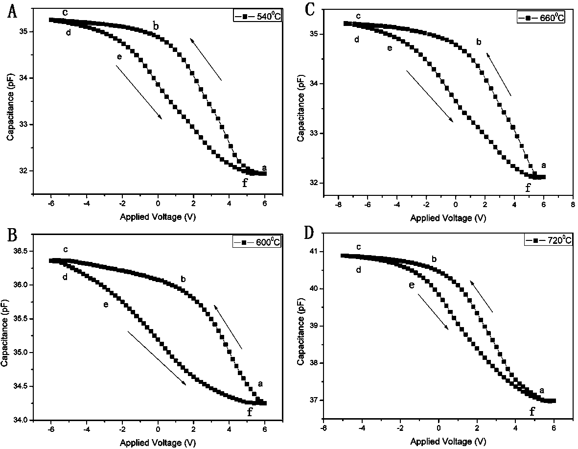
[0049] The element voltage-capacitance relationship characteristic prepared by embodiment 2-4 is detected, and the results are as follows: image 3 In A, C, and D, the statistical results of the size of the storage window are shown in Table 1.
[0050] In addition, the TEM scanning method was used to detect the generated SiO 2 The thickness of the tunneling layer, the results are shown in Table 1.
[0051] Table 1:
[0052]
[0053] Depend on image 3 , Figure 4 It can be seen from the statistical results in Table 1 that the storage element of the present invention is ideal as a whole in the annealing temperature range of 540-720°C, but as the annealing temperature increases, the SiO 2 The thickness of the tunneling layer also increases gradually. When the annealing temperature is 600°C, the thickness of the tunneling layer of the storage eleme...
Embodiment 5-12
[0055] Change Ga 2 o 3 Layer thickness and annealing temperature (see Table 2 for details), and other conditions are the same as in Example 1.
[0056] Table 2:
[0057]
[0058] It can be seen from the statistical results in Table 2 that Ga 2 o 3 The storage element made by layer thickness in the range of 35-65nm is generally ideal, but the Ga 2 o 3 When the layer thickness is about 50nm, the storage window of the storage element is the largest, and the storage performance is the best.
PUM
| Property | Measurement | Unit |
|---|---|---|
| thickness | aaaaa | aaaaa |
| thickness | aaaaa | aaaaa |
| thickness | aaaaa | aaaaa |
Abstract
Description
Claims
Application Information


