A kind of epitaxial wafer of light-emitting diode and its manufacturing method
A technology of light-emitting diodes and manufacturing methods, applied to semiconductor devices, electrical components, circuits, etc., can solve problems such as excessive stress, lattice mismatch, affecting device functions and reliability, etc., achieve good lattice matching, improve Crystal quality, effect of defect reduction
- Summary
- Abstract
- Description
- Claims
- Application Information
AI Technical Summary
Problems solved by technology
Method used
Image

Examples
Embodiment 1
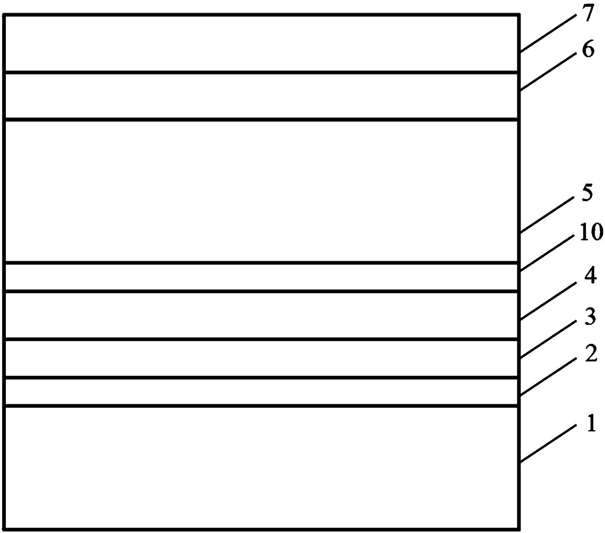
[0033] An embodiment of the present invention provides an epitaxial wafer of a light emitting diode, see figure 1 , the epitaxial wafer includes a sapphire substrate 1, and a buffer layer 2, a nucleation layer 3, an undoped GaN layer 4, an improvement layer 10, an N-type layer 5, an active layer 6, a P Type Layer 7.
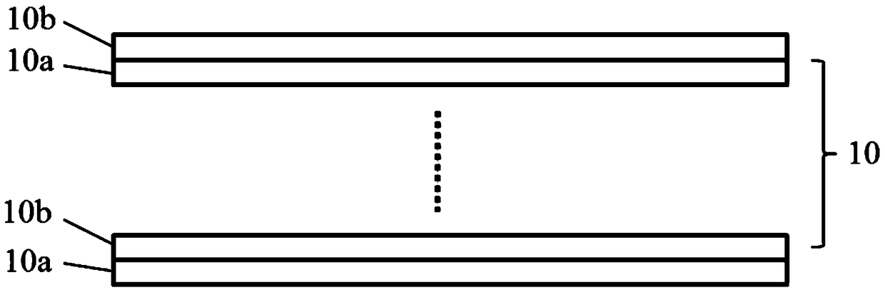
[0034] In this example, see figure 2 , the improved layer 10 may include alternately stacked SiN layers 10a and GaN layers 10b.
[0035] Optionally, the improved layer may include a first improved sub-layer, a second improved sub-layer, and a third improved sub-layer stacked in sequence, and the first improved sub-layer, the second improved sub-layer, and the third improved sub-layer all include alternately stacked SiN layer and GaN layer, the Si component content in the SiN layer in the first improved sublayer is higher than the Si component content in the SiN layer in the second improved sublayer, and the Si component content in the SiN layer in the second i...
Embodiment 2
[0042] An embodiment of the present invention provides a method for manufacturing an epitaxial wafer of a light emitting diode, which is suitable for manufacturing the epitaxial wafer provided in Embodiment 1. When it is realized, trimethylgallium or trimethylethane is used as the gallium source, high-purity NH3 is used as the nitrogen source, trimethylindium is used as the indium source, trimethylaluminum is used as the aluminum source, the N-type dopant is silane, and the P-type dopant is silane. Miscellaneous agent selects dichloromagnesium for use.
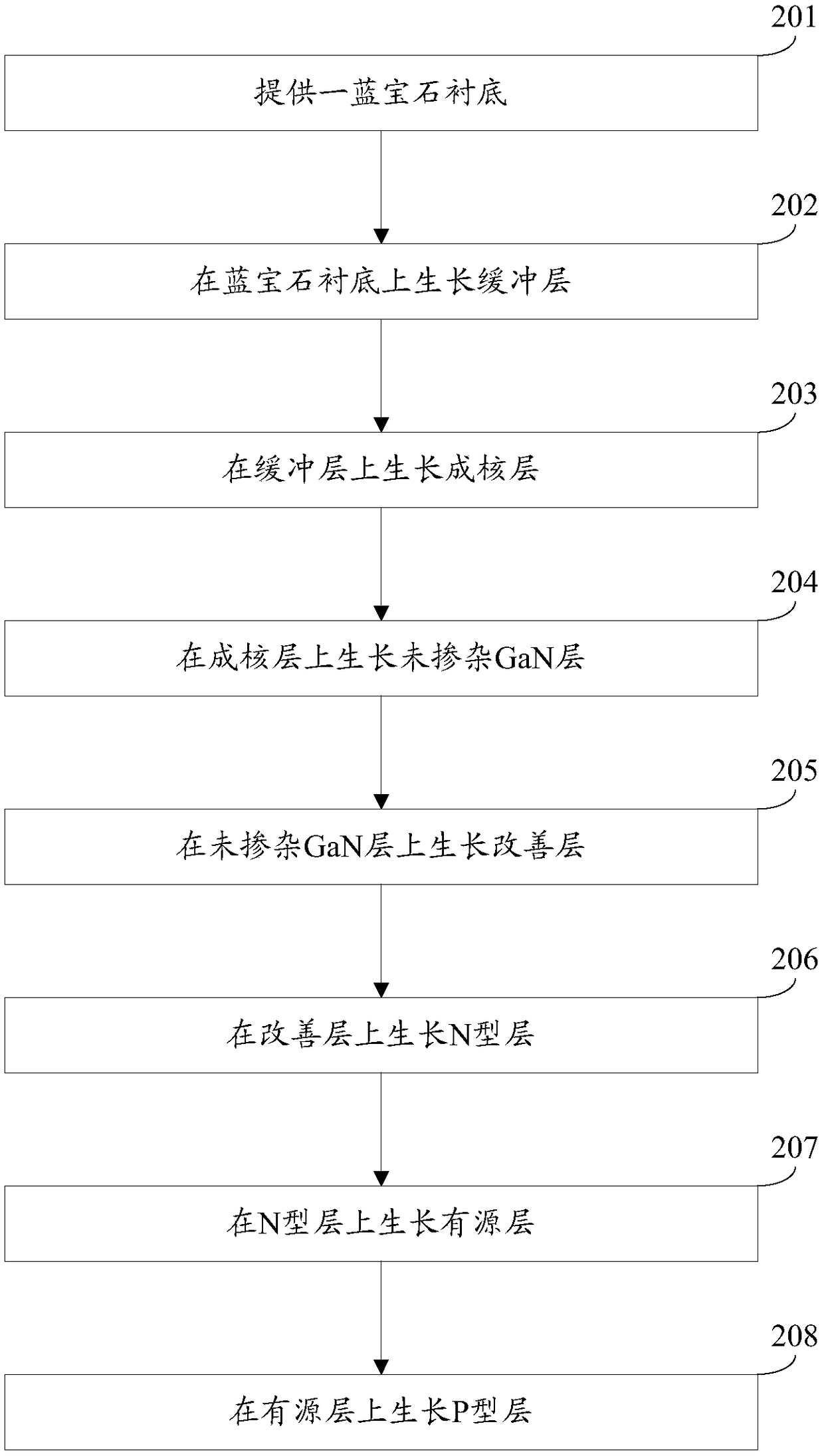
[0043] Specifically, see image 3 , the manufacturing method includes:
[0044] Step 201: Provide a sapphire substrate.
[0045]In a specific implementation, the sapphire substrate will be heated to 1060°C in a Metal Organic Chemical Vapor Deposition (English: MetaOrganic Chemical Vapor Deposition, MOCVD) reaction chamber first, and then the sapphire substrate will be annealed in a hydrogen atmosphere. , and finally carry o...
Embodiment 3
[0072] An embodiment of the present invention provides an epitaxial wafer of a light emitting diode, see Figure 4 , the epitaxial wafer includes a sapphire substrate 1, and a buffer layer 2, a nucleation layer 3, an undoped GaN layer 4, an N-type layer 5, an improvement layer 10, an active layer 6, a P Type Layer 7.
[0073] In this embodiment, the improved layer may be the same as the improved layer provided in Embodiment 1, which will not be described in detail here.
[0074] Specifically, the sapphire substrate may be the same as that provided in Embodiment 1, the buffer layer may be the same as that provided in Embodiment 1, the nucleation layer may be the same as that provided in Embodiment 1, and the undoped GaN The layer can be the same as the undoped GaN layer provided in Embodiment 1, the N-type layer can be the same as the N-type layer provided in Embodiment 1, the active layer can be the same as the active layer provided in Embodiment 1, and the P-type layer can b...
PUM
 Abstract
Description
Claims
Application Information
 - R&D
- Intellectual Property
- Life Sciences
- Materials
- Tech Scout
- Unparalleled Data Quality
- Higher Quality Content
- 60% Fewer Hallucinations
Browse by: Latest US Patents, China's latest patents, Technical Efficacy Thesaurus, Application Domain, Technology Topic, Popular Technical Reports.
© 2025 PatSnap. All rights reserved.Legal|Privacy policy|Modern Slavery Act Transparency Statement|Sitemap|About US| Contact US: help@patsnap.com