Micro gas chromatographic column chip with high aspect ratio and preparation method thereof
A micro gas chromatography and high aspect ratio technology, which is used in the field of separation of mixed gases and the preparation of high aspect ratio micro gas chromatography columns, can solve the problems of difficulty in increasing the aspect ratio of the channel, uneven heating on one side, and achieve the thermal expansion coefficient. Consistent, enhanced separation and resolution, strong bonding results
- Summary
- Abstract
- Description
- Claims
- Application Information
AI Technical Summary
Problems solved by technology
Method used
Image
Examples
preparation example Construction
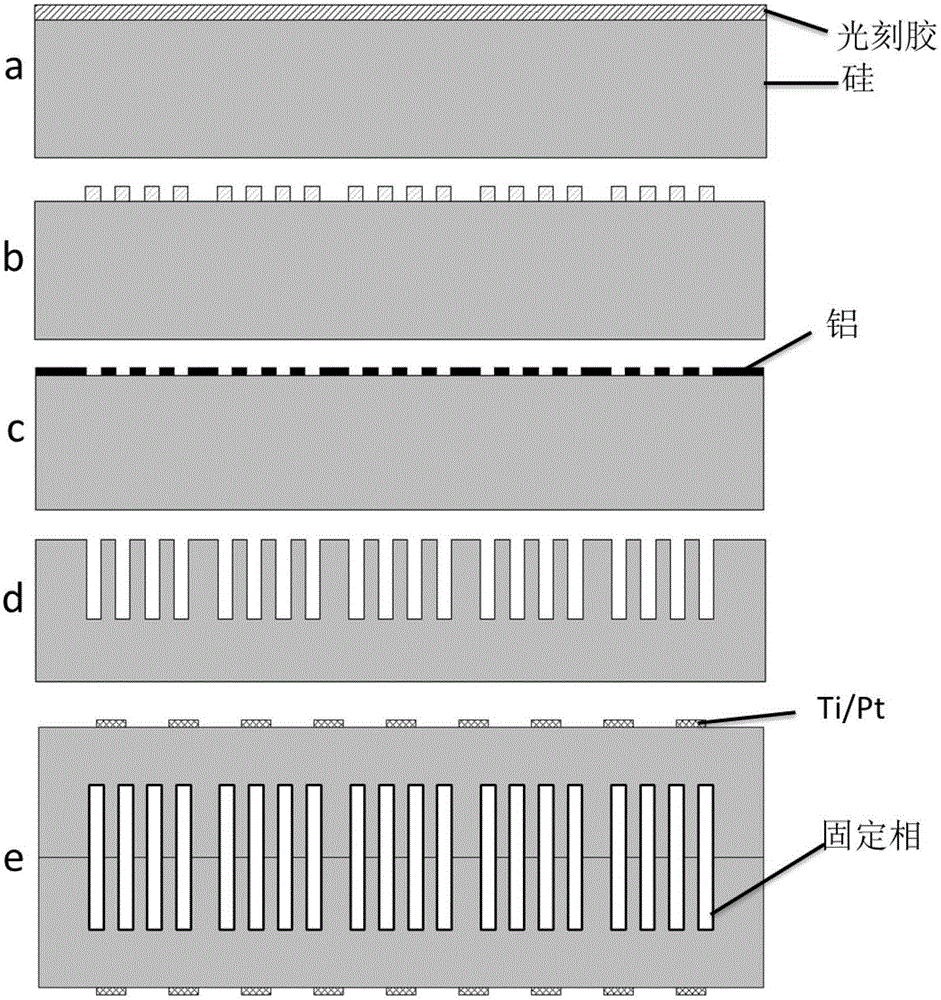
[0035] image 3 (a)-(e) are process flow charts of the method for preparing a high aspect ratio micro gas chromatographic column chip according to an embodiment of the present invention. Include the following steps:
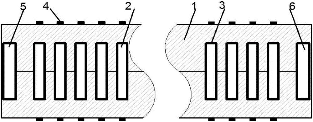
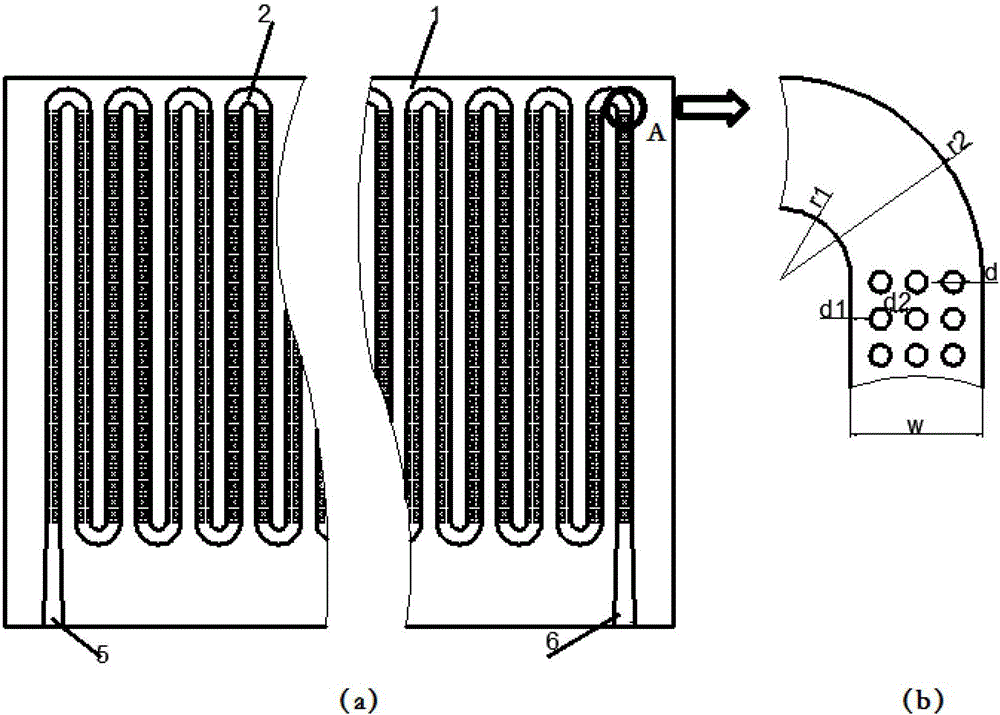
[0036] 1) Design and manufacture mask plate: according to figure 1 , 2 The structure of the design shown, fabricated on a glass substrate figure 1 , 2 (a)-(b) shows a continuous serpentine channel, in which circular columns are arranged in an array, and the spacing of the columns is symmetrically and unequally spaced.
[0037] 2) Silicon wafer pretreatment: clean the silicon wafer, place the silicon wafer in a mixed solution of concentrated sulfuric acid and hydrogen peroxide solution heated at 100-120°C in a volume ratio of 3:1, and clean it for 5-8 minutes. Rinse well and blow dry with air, then dry the silicon.
[0038] 3) Photolithography: choose a polished silicon wafer with a thickness of 500 μm as the silicon substrate, and then spin-coat photoresist...
Embodiment 1
[0046] Place the silicon wafer in a solution heated at 120°C, concentrated sulfuric acid and hydrogen peroxide solution at a volume ratio of 3:1, wash for 5 minutes, rinse with deionized water, dry with air, and then bake at 90°C Dry the silicon wafer for 10 minutes. Spin-coat photoresist N244 on the silicon wafer, place the silicon wafer with spin-coated photoresist on a heating plate at 95° C. for 5 minutes, and dry it.
[0047] Place the dried silicon wafer on the photolithography table, align the mask plate and stick it to the silicon wafer, set the exposure time to 6s, and immediately place the exposed silicon wafer on a heating plate at 120°C for intermediate baking. The time is 3 minutes, and then the silicon wafer is placed in 2.5% tetramethylammonium hydroxide solution for development, and the development time is 30s. After development, it can be seen that the pattern of the mask plate has been transferred to the silicon wafer. Dry the wafer for 10 min.
[0048] A m...
Embodiment 2
[0052] Place the silicon wafer in a solution heated at 100°C, concentrated sulfuric acid and hydrogen peroxide solution at a volume ratio of 3:1 and wash for 8 minutes, rinse with deionized water, dry with air, and then bake at 85°C Dry the silicon wafer for 10 minutes. Spin-coat photoresist N244 on the silicon wafer, place the silicon wafer with spin-coated photoresist on a heating plate at 85° C. for 8 minutes, and dry it.
[0053] Place the dried silicon wafer on the photolithography table, align the mask plate and stick it to the silicon wafer, set the exposure time for 5s, and immediately place the exposed silicon wafer on a heating plate at 110°C for intermediate baking. The time is 5 minutes, and then the silicon wafer is placed in a 2.5% tetramethylammonium hydroxide solution for development, and the development time is 25 seconds. After development, it can be seen that the pattern of the mask plate has been transferred to the silicon wafer. Dry the wafer for 15 minut...
PUM
| Property | Measurement | Unit |
|---|---|---|
| Thickness | aaaaa | aaaaa |
| Wall thickness | aaaaa | aaaaa |
| Diameter | aaaaa | aaaaa |
Abstract
Description
Claims
Application Information


