Ultraviolet avalanche photodiode detector and detection method thereof

A photodiode and avalanche diode technology, which is applied in the use of electrical radiation detectors for photometry, circuits, electrical components, etc., can solve the problems of large dark excitation and dark current noise, large avalanche area, and low detection efficiency. The effect of improving frequency response, improving detection efficiency, and improving quantum efficiency

Inactive Publication Date: 2017-05-31
BEIJING CENTURY GOLDRAY SEMICON CO LTD
View PDF4 Cites 9 Cited by
  • Summary
  • Abstract
  • Description
  • Claims
  • Application Information

AI Technical Summary

Problems solved by technology

The low detection efficiency of the existing ultraviolet APD is mainly due to its large avalanche area, large dark excitation and dark current noise, and low signal-to-noise ratio.

Method used


Image

  • Ultraviolet avalanche photodiode detector and detection method thereof

Examples


Embodiment Construction

[0023] The present invention will now be described more fully with reference to the accompanying drawings, in which exemplary embodiments of the invention are shown. This invention may, however, be embodied in many different forms and should not be construed as limited to the exemplary embodiments set forth herein. Rather, these embodiments are provided so that this disclosure will be thorough and complete, and will fully convey the scope of the invention to those skilled in the art.

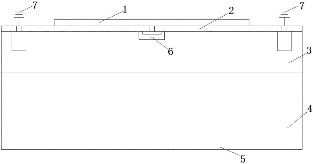
[0024] Such as figure 1 As shown, the present invention provides a UV avalanche photodiode detector, each device unit of the detector includes CE (Collecting electrode) electrode 1, SiO 2 Layer 2, P-well or N-well3, substrate 4, and back electrode 5; wherein, the upper center of P-well or N-well3 is provided with a dotted avalanche diode 6, and the dotted avalanche diode 6 is electrically connected to the CE electrode 1; SiO 2 A ground GND7 is provided on the periphery of layer 2 in the circu...


PUM


Abstract

The invention discloses an ultraviolet avalanche photodiode detector. Each device unit of the detector comprises a CE electrode, an SiO2 layer, a P-well or N-well, a substrate and a back surface electrode in sequence from top to bottom, wherein a point-shaped avalanche photodiode is arranged at the center of the upper part of the P-well or N-well; the point-shaped avalanche photodiode is electrically communicated with the CE electrode; a ground connector GND is peripherally arranged at the periphery of the SiO2 layer. The ultraviolet avalanche photodiode detector is manufactured by adopting a wide band gap semiconductor material, an avalanche region is separated from a photon collection region, and an avalanche multiplication nodal region is relatively small, so that a device with relatively low avalanche voltage can be manufactured, and the uniformity and controllability of an electric field of the avalanche region are good; while an avalanche multiplication high-field region is relatively small, a large-area optical detection region is guaranteed, so that the quantum efficiency is improved; the area of the avalanche region is reduced, and dark current and dark excitation are easy to reduce; meanwhile, the tolerance to the quality and defects of a wafer is improved, and breakdown of the large-area avalanche multiplication high-field region at a defect position is prevented in advance.

Description

technical field [0001] The invention belongs to the field of H01L 27 / 00 semiconductor devices, and in particular relates to an ultraviolet avalanche photodiode detector with a field plate drift structure and a detection method thereof. Background technique [0002] Avalanche Photodiode Detector (APD) for low light detection. The ultraviolet light detector with "solar blindness" characteristic made of third-generation wide-bandgap semiconductor materials (such as SiC, GaN, etc.) can work at high temperature without expensive and bulky refrigeration system, and is resistant to radiation High near-UV response. Because of its excellent characteristics in aerospace, astronomical exploration and military affairs, it has always been a research hotspot. [0003] Compared with traditional photomultiplier tubes, ultraviolet APD has the advantages of single photon response, large gain, insensitivity to magnetic field, simple manufacturing process, low cost, small size, easy CMOS proc...

Claims


Application Information

Patent Timeline
Patent Type & Authority Applications(China)
IPC IPC(8): H01L31/0224H01L31/0312H01L31/0352H01L31/107G01J1/42
CPCH01L31/107G01J1/42H01L31/022408H01L31/022475H01L31/0312H01L31/03529
Inventor 袁俊倪炜江张敬伟李明山牛喜平季莎徐妙玲
Owner BEIJING CENTURY GOLDRAY SEMICON CO LTD
Why Eureka
Try Eureka