Photovoltaic near and middle infrared double-color detector for Si-based three-dimensional Ge quantum dot crystal

A technology of two-color detectors and quantum dots, applied in photovoltaic power generation, semiconductor devices, electrical components, etc., can solve the problems of high material cost, difficult preparation, on-chip integration of photosensitive elements, etc., and achieve high detection rate, strong light absorption coefficient, The effect of improving overall performance

Inactive Publication Date: 2017-06-13
SHANGHAI INST OF MICROSYSTEM & INFORMATION TECH CHINESE ACAD OF SCI
View PDF5 Cites 9 Cited by
  • Summary
  • Abstract
  • Description
  • Claims
  • Application Information

AI Technical Summary

Problems solved by technology

[0004] At present, the mainstream two-color infrared detector products are all made of III-V compound semiconductor materials or Si combined with III-V semiconductor materials. Although the devices have the advantages of high quantum efficiency and high sensitivity, they also have high material costs, preparation difficulties
In addition, almost all current infrared focal plane readout circuits are Si-based integrated circuits, and III-V photosensitive elements cannot be directly integrated with Si on-chip, so it is necessary to use technologies such as indium pillar flip-bonding packaging to integrate photosensitive elements with Si readouts. out of the circuit for coupling to enable imaging applications

Method used


Image

  • Photovoltaic near and middle infrared double-color detector for Si-based three-dimensional Ge quantum dot crystal
  • Photovoltaic near and middle infrared double-color detector for Si-based three-dimensional Ge quantum dot crystal
  • Photovoltaic near and middle infrared double-color detector for Si-based three-dimensional Ge quantum dot crystal

Examples


Embodiment 1

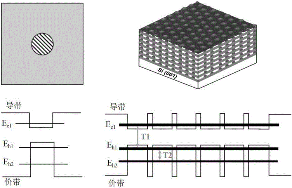
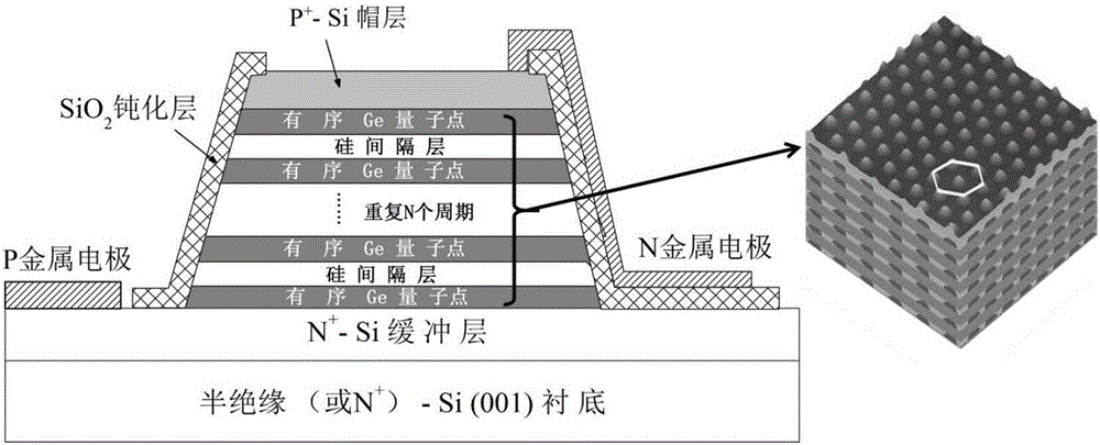
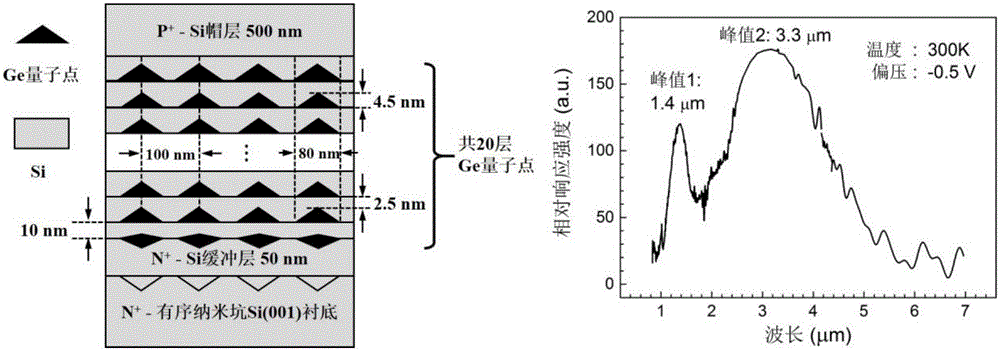
[0032] The purpose of this embodiment is to prepare a three-dimensional Ge quantum dot crystal two-color detector whose response wavelength covers the near-middle infrared band on a Si substrate. The preparation of Ge quantum dot crystals is achieved by growing Ge quantum dot arrays ordered in three dimensions by molecular beam epitaxy on a Si(001) pattern substrate etched with two-dimensional ordered arrangements. The in-plane order of Ge quantum dots is realized by the positioning and growth of pre-etched nanopits, while the order in the vertical direction is realized by the strain self-alignment effect of Ge quantum dots during multilayer stack growth. The size of Ge quantum dots is regulated by optimizing the growth conditions. Near-neighbor strong coupling of in-plane Ge QDs is achieved by reducing the period of the nanopit. The strong coupling of Ge quantum dots in the vertical direction is achieved by reducing the thickness of the Si spacer layer between adjacent Ge qu...


PUM


Abstract

The invention relates to a photovoltaic near-infrared and middle-infrared double-color detector for an Si-based three-dimensional Ge quantum dot crystal. The detector structure is a photovoltaic light-emitting diode structure of a PIN or NIP structure, wherein the three-dimensional Ge quantum dot crystal serves as a light absorption region. Strong near-infrared and middle-infrared band light absorption is formed by using efficient ground state micro-strip interband transition and valence band micro-strip sub-band interband transition inside the three-dimensional Ge quantum dot crystal, so that efficient double-color detection for near-infrared and middle-infrared wave bands is realized simultaneously, and the photovoltaic near and middle infrared double-color detector has wide application prospect in the technical field of infrared sensing.

Description

technical field [0001] The invention belongs to the field of semiconductor infrared detection materials and devices, in particular to a Si-based three-dimensional Ge quantum dot crystal photovoltaic type near-middle infrared two-color detector. Background technique [0002] Since the earth's atmospheric environment has a specific strong absorption band for infrared rays, only infrared radiation with wavelengths between 1-2.5 μm, 3-5 μm and 8-14 μm can be effectively transmitted and detected in the atmospheric environment. These three bands are the so-called three atmospheric windows of near-infrared, mid-infrared and far-infrared. Traditional infrared detectors, such as short-wave infrared InGaAs, medium-wave infrared InSb, and long-wave infrared HgCdTe, etc., although they can provide enhanced detection sensitivity by preparing PIN photovoltaic, photoconductive, and avalanche structures, each detector Each of the detection light bands can only cover one infrared atmospheri...

Claims


Application Information

Patent Timeline
Patent Type & Authority Applications(China)
IPC IPC(8): H01L31/028H01L31/0352H01L31/105
CPCH01L31/028H01L31/035218H01L31/1055Y02E10/547
Inventor 马英杰张永刚
Owner SHANGHAI INST OF MICROSYSTEM & INFORMATION TECH CHINESE ACAD OF SCI
Why Eureka
Try Eureka