

P-i-n-type antimony selenide thin-film solar cell
A technology of solar cells and antimony selenide, which is applied in the field of solar cells, can solve problems such as low performance and interface defects of antimony selenide solar cells, achieve the effects of reducing high recombination rate, reducing lattice mismatch degree, and broad application prospects
- Summary
- Abstract
- Description
- Claims
- Application Information
AI Technical Summary
Problems solved by technology
Method used
Image

Examples
Embodiment 1
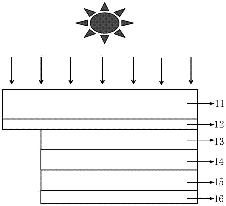
[0022] Such as figure 1 As shown, the structure of the p-i-n type solar cell provided in this embodiment from top to bottom is (along the light direction) glass substrate 11, ITO transparent conductive top electrode layer 12, p-type antimony selenide semiconductor layer 13, intrinsic ZnO semiconductor i-type layer 14 , n-type Ag-doped antimony selenide semiconductor layer 15 and Au bottom electrode layer 16 .
[0023] Concrete preparation steps are as follows:
[0024] (1) Clean the substrate
[0025] Using soda-lime glass as the substrate, the glass was first soaked in electronic cleaner solution for 15 min, then it was taken out, rinsed with plenty of deionized water, and finally blown dry with nitrogen.
[0026] (2) Deposition of ITO transparent conductive top electrode layer
[0027] Use magnetron sputtering technology to deposit ITO transparent conductive top electrode layer (indium tin oxide semiconductor transparent conductive film): fix the cleaned glass substrate o...
Embodiment 2
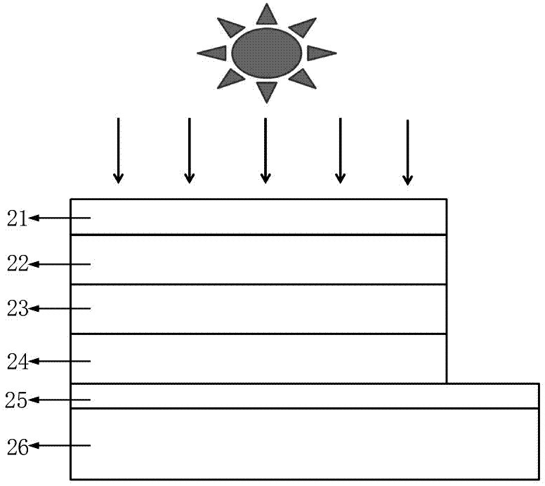
[0037] Such as figure 2 As shown, the structure of the p-i-n type solar cell provided by this embodiment from top to bottom is (along the light direction BZO top electrode layer 21, p-type antimony selenide semiconductor layer 22, intrinsic antimony selenide semiconductor i-type layer 23. An n-type Cu-doped antimony selenide semiconductor layer 24 , a Mo bottom electrode layer 25 and a stainless steel substrate 26 .
[0038] Concrete preparation steps are as follows:
[0039] (1) Clean the substrate
[0040] Using stainless steel as the substrate, first soak the stainless steel substrate in the electronic cleaner solution for 15 min, then take it out, rinse it with a large amount of deionized water, and dry it with nitrogen.
[0041] (2) Deposit Mo bottom electrode layer
[0042] Using magnetron sputtering technology to deposit Mo (molybdenum) bottom electrode layer: fix the cleaned stainless steel substrate on the support, put it into a vacuum chamber, and the vacuum degr...
Embodiment 3
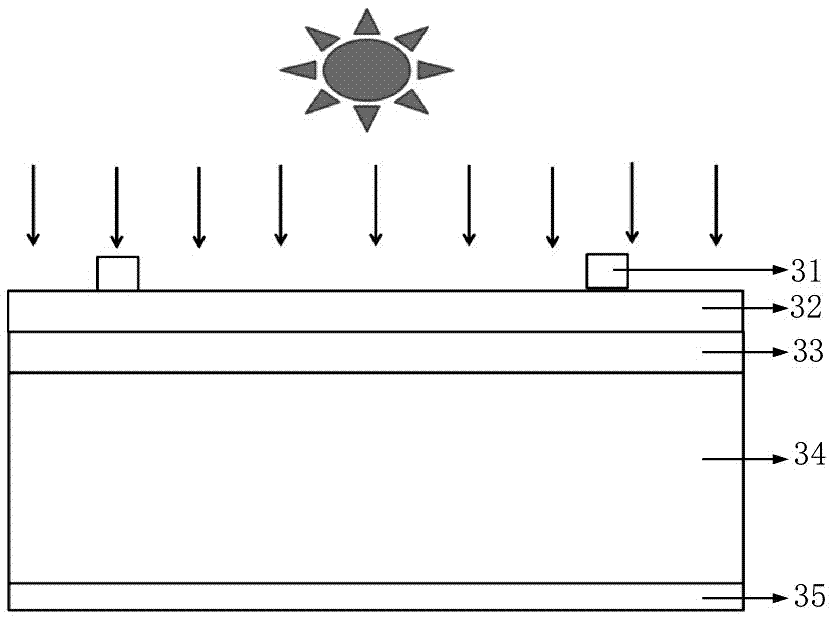
[0052] Such as image 3 As shown, the structure of the p-i-n type solar cell provided in this embodiment from top to bottom is (along the light direction) Ag top electrode layer 31, p-type sulfur-doped antimony selenide semiconductor layer 32, intrinsic amorphous silicon semiconductor layer i-type layer 33 , n-type Ag-doped antimony selenide single crystal layer 34 and Ag bottom electrode layer 35 .
[0053] Concrete preparation steps are as follows:
[0054] (1) Preparation of n-type Ag-doped antimony selenide single crystal layer
[0055] The n-type Ag-doped antimony selenide single crystal layer with a thickness of 1-100 μm is prepared by Czochralski method, zone melting method or directional solidification method, and it can also be grown and prepared by epitaxial method. Wherein the molar ratio of selenium, antimony and Ag is 3:2:0.001-0.01.
[0056] (2) Deposition of intrinsic amorphous silicon semiconductor i-type layer
[0057] The intrinsic amorphous silicon semic...
PUM
| Property | Measurement | Unit |
|---|---|---|
| Thickness | aaaaa | aaaaa |
| Thickness | aaaaa | aaaaa |
| Thickness | aaaaa | aaaaa |
Abstract
Description
Claims
Application Information