Micro-display OLED device and manufacturing method thereof

A micro-display and device technology, applied in semiconductor/solid-state device manufacturing, electric solid-state devices, semiconductor devices, etc., can solve problems such as improving yield rate, simplifying process, and improving yield rate, so as to improve yield rate, simplify process, improve performance effect

Inactive Publication Date: 2017-07-18
CHENGDU JINGSHA TECH
View PDF4 Cites 6 Cited by
  • Summary
  • Abstract
  • Description
  • Claims
  • Application Information

AI Technical Summary

Problems solved by technology

First of all, the anode needs to have a high light reflectivity, so the ITO material used in the OLED on the glass substrate cannot be directly used. It is necessary to develop a new anode material and use a multi-layer composite anode film, and in the traditional silicon-based micro-display OLED process In the method, the above-mentioned anode is manufactured in the OLED factory first after coating and then photoetching the pixel pattern, which not only requires additional investment in the OLED factory to supplement the anode coating and photolithography equipment, but also requires the use of a photolithography process. This wet process is the same as The vacuum evaporation dry process used to make other OLED structural layers is incompatible, which increases the complexity of the process and is not conducive to improving the yield; although there are also research papers that propose that the anode should be made in an integrated circuit wafer foundry, However, the metals such as Al and Cu that can be used in the standard CMOS process do not meet the requirements of OLEDs for anode materials with high work functions, resulting in higher driving voltage and higher power consumption for OLEDs, and a decline in luminous performance.
Secondly, the cathode in the above silicon-based micro-display OLED device structure must use a metal transparent cathode, which is not only difficult to choose a suitable metal material but also requires a very thin metal layer. The thinner the metal cathode, the better the light transmission, but the greater the impedance, The higher the power consumption, the current transparent cathode technology is not yet mature in the OLED industry
Therefore, using the above-mentioned traditional silicon-based micro-display OLED device structure, generally the anode and cathode need to use multi-layer composite films of various metals or metal oxides, which face great challenges in material selection and manufacturing process, which is not conducive to simplifying the manufacturing process. , improve yield rate, reduce cost, improve performance

Method used


Image

  • Micro-display OLED device and manufacturing method thereof
  • Micro-display OLED device and manufacturing method thereof
  • Micro-display OLED device and manufacturing method thereof

Examples


Embodiment 1

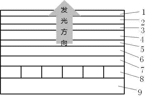
[0028] Embodiment one Figure 4 Shown is the device structure of the single-color (such as a certain display color such as green, blue or yellow) or white silicon-based micro-display OLED described in the present invention, and a protective glass is added outside the thin-film encapsulation layer. Among them, the cathode is metal Al, and the small squares in the cathode in the figure indicate the pixel pattern. Both the cathode coating and the cathode pixel pattern are manufactured in the integrated circuit wafer foundry using the standard CMOS process; the light-emitting layer EML emits the required green, blue , yellow or white organic light-emitting material layer; the anode is the most commonly used ITO transparent conductive oxide in the flat panel display industry, which not only has good light transmission and conductivity, but also has a high work function, and is easy to integrate with the hole injection layer, etc. Organic materials achieve the best energy level matc...

Embodiment 2

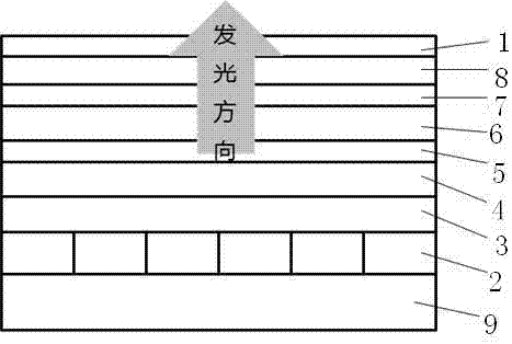
[0029] Embodiment two Figure 5 Shown is the device structure of the full-color silicon-based micro-display OLED of the present invention, in which a color filter film CF and a protective glass are added outside the thin film encapsulation layer. The cathode is metal Mg, and the small squares on the cathode in the figure indicate the pixel pattern. Both the cathode coating and the cathode pixel pattern are manufactured in the integrated circuit wafer foundry using a standard CMOS process; the light-emitting layer EML is an organic light-emitting material layer that emits white light ; The anode is the most commonly used ITO transparent conductive oxide in the flat panel display industry. It not only has good light transmission and conductivity, but also has a high work function, and is easy to achieve the best energy level matching with organic materials such as hole injection layers. , in order to reduce the driving voltage of OLED and improve the luminous performance, the IT...


PUM


Abstract

The invention discloses a micro-display OLED device which comprises the components of a CMOS circuit, a cathode, an electron injection layer (EIL), an electron transportation layer (ETL), a light emitting layer (EML), a hole transport layer (HTL), a hole injection layer (HIL), an anode and a packaging film layer. The cathode, the electron injection layer (EIL), the electron transportation layer (ETL), the light emitting layer (EML), the hole transportation layer (HTL), the hole injection layer (HIL), the anode and the packaging film layer are successively arranged on the CMOS circuit. Light which is emitted from the light emitting layer is transmitted in the anode direction. According to the micro-display OLED device structure and the manufacturing method thereof, the silicon-base micro-display OLED can be composed of an anode material and a cathode material which are same with the anode material and the cathode material of the OLED on a glass substrate; and furthermore the OLED is perfectly combined with a CMOS process, thereby simplifying manufacture process of the silicon-base micro-display OLED, improving yield, reducing cost and improving performance.

Description

technical field [0001] The invention belongs to the field of display technology, and in particular relates to a device structure of an organic light emitting diode (OLED) and a manufacturing method thereof. Background technique [0002] Organic light-emitting diode (OLED) display is recognized by the industry as the third-generation display technology after liquid crystal display (LCD) due to its thinness, active light emission, fast response speed, wide viewing angle, rich colors, high and low temperature resistance and many other advantages. It can be widely used in terminal products such as VR / AR (virtual reality / augmented reality), smartphones, tablet computers, TVs, and military helmet displays. [0003] Micro-display OLED display device refers to an organic light-emitting display device with a display size of less than 1 inch and driven by silicon-based CMOS. It is a perfect combination of CMOS technology and OLED technology. / Key component of camera viewfinder. At ...

Claims


Application Information

Patent Timeline
Patent Type & Authority Applications(China)
IPC IPC(8): H01L27/32H01L51/52H01L51/56
CPCH10K59/38H10K50/81H10K71/00
Inventor 田国军黎守新
Owner CHENGDU JINGSHA TECH
Why Eureka
Try Eureka