P-type PERC double-faced solar cell employing laser marking alignment and preparation method thereof

A solar cell and laser marking technology, applied in the field of solar cells, can solve the problems of defective rate of double-sided PERC solar cells, inaccurate printing of aluminum paste, inaccurate positioning, etc. Effect

Active Publication Date: 2017-07-21
ZHEJIANG AIKO SOLAR ENERGY TECH CO LTD
View PDF8 Cites 12 Cited by
  • Summary
  • Abstract
  • Description
  • Claims
  • Application Information

AI Technical Summary

Problems solved by technology

However, this silicon wafer edge alignment method has the following defects: there will be errors in the silicon wafer manufacturing process, so that its shape may not be a standard square shape, and the silicon wafer edge alignment method will cause inaccurate positioning. , this is because the printing machine determines the position of the aluminum paste to be printed according to the distance between the edge of the silicon wafer and the laser grooved area during printing, and the shape of the silicon wafer is not a regular square, which directly leads to the back of each silicon wafer The aluminum paste cannot be printed accurately on the laser grooved area, which increases the defect rate of double-sided PERC solar cells

Method used


Image

  • P-type PERC double-faced solar cell employing laser marking alignment and preparation method thereof
  • P-type PERC double-faced solar cell employing laser marking alignment and preparation method thereof
  • P-type PERC double-faced solar cell employing laser marking alignment and preparation method thereof

Examples


Embodiment 1

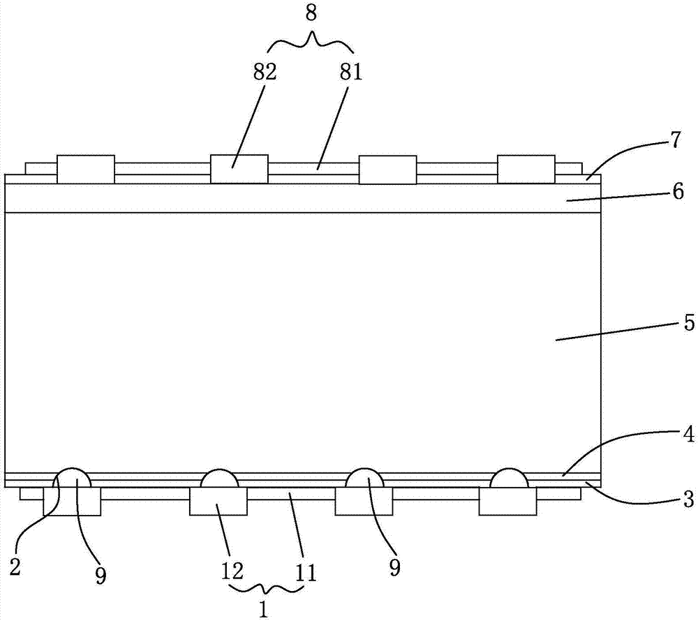
[0044] Such as figure 1 and 2As shown, it is a P-type PERC double-sided solar cell that adopts laser marking alignment according to the present invention, including a back electrode 1, a back silicon nitride film 3, an aluminum oxide film 4, a P-type silicon 5, The N-type emitter 6, the front silicon nitride film 7 and the front silver electrode 8, the front silver electrode 8 is mainly formed by connecting the front silver electrode sub-grid 82 and the front silver electrode main grid 81 which are vertically intersecting. The back silver electrode 1 is mainly formed by connecting the back main grid line 11 and the back aluminum grid line 12 which are vertically intersecting. On the back silicon nitride film 3, there are several holes penetrating the back silicon nitride film 3 and the aluminum oxide film 4. Groove 2 constitutes laser grooved area 10, P-type silicon 5 is exposed in groove 2, the part 9 of back aluminum gate line 12 located in groove 2 is connected with P-type...

Embodiment 2

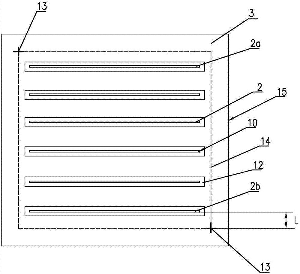
[0059] Such as image 3 As shown, the difference between this embodiment and Embodiment 1 is that there are four laser marks 13 located at the four corners of the solar cell 15 , and all the laser marks 13 are located on the same square 14 .

[0060] A method for preparing the above-mentioned P-type PERC double-sided solar cell using laser marking alignment, comprising the following steps:

[0061] (1) Form a suede surface on the front side of the P-type silicon 5;

[0062] (2) Diffusion is performed on the front side of the product obtained in step (1) to form an N-type emitter 6;

[0063] (3) Remove the phosphosilicate glass and surrounding PN junctions formed by the product obtained in step (2) during the diffusion process, and after polishing the back, turn to step (4);

[0064] (4) Deposit an aluminum oxide film 4 and a silicon nitride film 3 on the back in sequence on the back side of the product obtained in step (3), and then deposit a front silicon nitride film 7 on ...

Embodiment 3

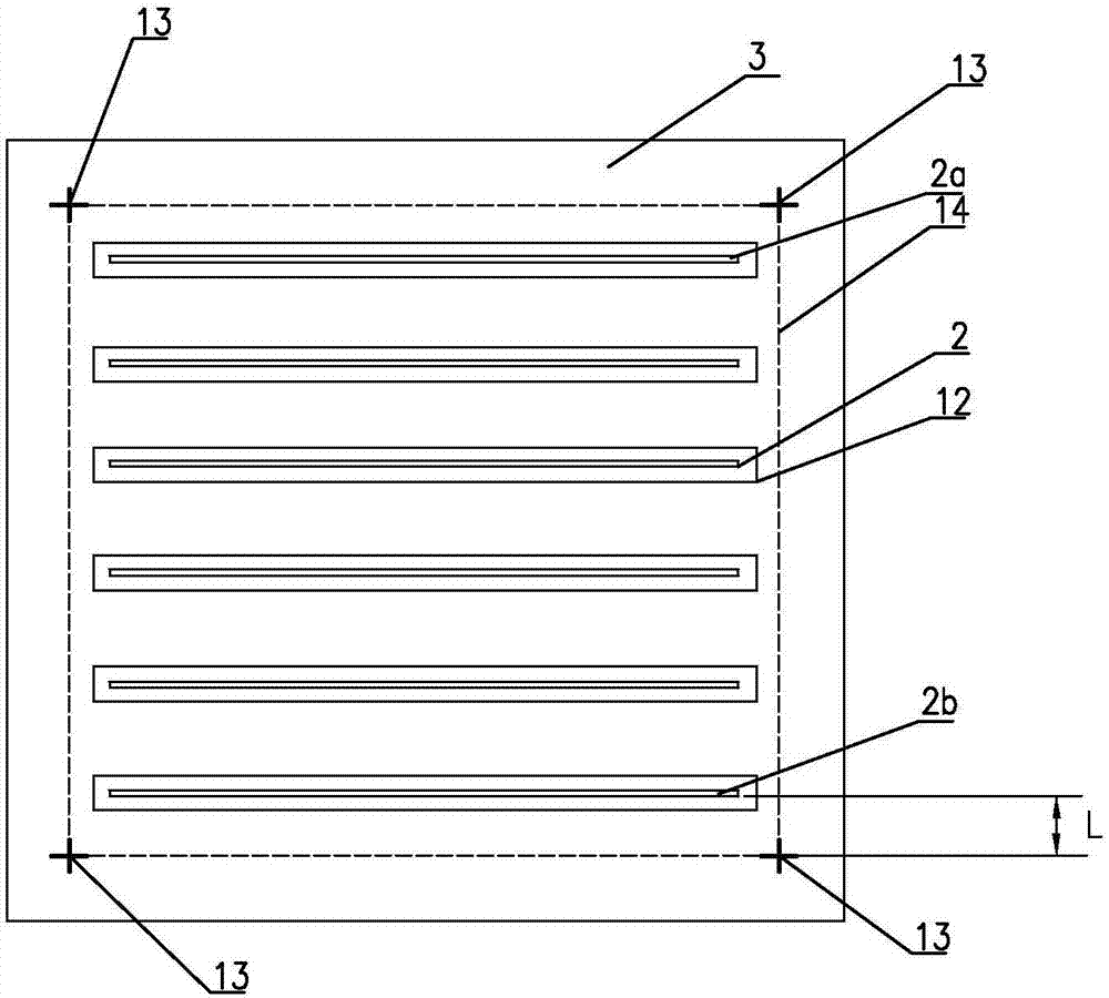
[0072] Such as Figure 4 As shown, the difference between this embodiment and Embodiment 1 is that there are two laser marks 13 , which are respectively close to opposite sides of the solar cell 15 , and all the laser marks 13 are located on the same square 14 .

[0073] A method for preparing the above-mentioned P-type PERC double-sided solar cell using laser marking alignment, comprising the following steps:

[0074] (1) Form a suede surface on the front side of the P-type silicon 5;

[0075] (2) Diffusion is performed on the front side of the product obtained in step (1) to form an N-type emitter 6;

[0076] (3) Remove the phosphosilicate glass and surrounding PN junctions formed by the product obtained in step (2) during the diffusion process, and after polishing the back, turn to step (4);

[0077] (4) Deposit an aluminum oxide film 4 and a silicon nitride film 3 on the back in sequence on the back side of the product obtained in step (3), and then deposit a front silic...


PUM

PropertyMeasurementUnit
thicknessaaaaaaaaaa
thicknessaaaaaaaaaa

Abstract

The invention discloses a P-type PERC double-faced solar cell employing laser marking alignment and a preparation method thereof. The P-type PERC double-faced solar cell comprises back electrodes, a back side silicon nitride film, an alumina film, P-type silicon, an N-type emitter electrode, a front side silicon nitride film and positive silver electrodes which are sequentially arranged from bottom to top. Each back electrode is formed by a back electrode main grid and a back aluminum grid line which are vertically crossed and are connected with each other, the back side silicon nitride film is provided with several grooves traversing the back side silicon nitride film and the alumina film to form laser grooving zones, the P-type silicon is exposed in the grooves, the parts, of the back aluminum grid lines, arranged in the grooves are connected with the P-type silicon, the back side silicon nitride film is provided with laser marks, relative positions of the laser marks and the laser grooving zones are preset, by positioning the laser marks and in dependence on the distance between the laser grooving zones and the laser marks, the printing back aluminum grid lines are aligned. According to the invention, aluminium paste on the back side of each silicon chip can accurately cover the laser grooving zones, and the fraction defective of the double-faced PERC solar cells can be effectively reduced.

Description

technical field [0001] The invention relates to solar cell technology, in particular to a P-type PERC double-sided solar cell that adopts laser marking alignment, and also relates to a preparation method of the solar cell. Background technique [0002] A crystalline silicon solar cell is a device that effectively absorbs solar radiation energy and converts light energy into electrical energy by using the photovoltaic effect. When sunlight shines on the semiconductor P-N junction, new hole-electron pairs will be formed. Under the action of the electric field of the P-N junction, the holes flow from the N region to the P region, and the electrons flow from the P region to the N region. After the circuit is turned on A current is formed. [0003] Traditional crystalline silicon solar cells generally only use front passivation technology, that is, a layer of silicon nitride is deposited on the front of the silicon wafer by PECVD to reduce the recombination rate of minority carr...

Claims


Application Information

Patent Timeline
Patent Type & Authority Applications(China)
IPC IPC(8): H01L31/0216H01L31/068H01L31/18
CPCH01L31/02167H01L31/0684H01L31/1804Y02E10/547Y02P70/50
Inventor 林纲正方结彬陈刚
Owner ZHEJIANG AIKO SOLAR ENERGY TECH CO LTD
Why Eureka
Try Eureka