Manufacture method of metal nano circuit patterns based on DNA nano structures

A technology of metal nano and circuit patterns, applied in the direction of nanostructure manufacturing, specific nanostructure formation, nanotechnology, etc., can solve the problems of high cost and complicated application of photolithography technology, and achieve easy standardization, good biocompatibility, location highly specific effect

Active Publication Date: 2017-08-18
SHANGHAI INST OF APPLIED PHYSICS - CHINESE ACAD OF SCI
View PDF4 Cites 6 Cited by
  • Summary
  • Abstract
  • Description
  • Claims
  • Application Information

AI Technical Summary

Problems solved by technology

[0005] The purpose of the present invention is to provide a method for preparing metal nanocircuit patterns based on DNA nanostructures, so as to solve the problem that the application of photolithography technology becomes more and more complicated when the size of integrated circuit components is smaller than 100nm in the prior art. , and the cost is getting higher and higher

Method used


Image

  • Manufacture method of metal nano circuit patterns based on DNA nano structures
  • Manufacture method of metal nano circuit patterns based on DNA nano structures
  • Manufacture method of metal nano circuit patterns based on DNA nano structures

Examples


Embodiment 1

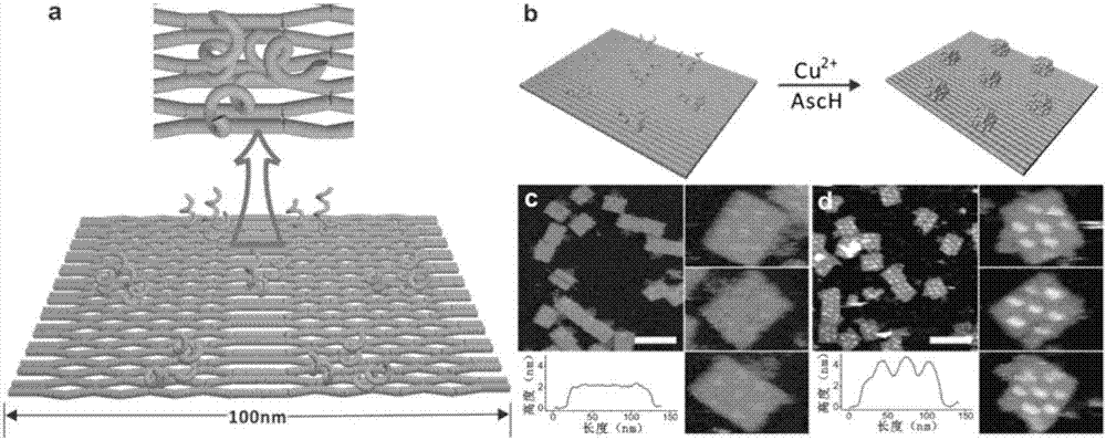
[0036] Example 1: Seed-free, selective copper metallization with nanometer-scale resolution by introducing "seven-dot" defect patterns on DNA origami by extending staple chains

[0037] Preparation of defect-introduced DNA origami: All required staple strands (including 5'-end extension single-stranded DNA as defective staple strand and normal staple strand without extension) were mixed with M13 long strand at a ratio of 10:1 Mixed at a ratio of 1 x TAE-Mg 2+ Buffer (tris, 40mM; acetic acid, 20mM; EDTA, 2mM; and magnesium acetate, 12.5mM; pH8.0) was annealed to synthesize DNA origami. The annealing process is the process reported in references (Rothemund, P.W.R. Nature 2006, 440, 297-302): the sample is slowly cooled from 95°C to 20°C at a rate of 1°C per minute.

[0038] Experimental procedure for selective Cu metallization with nanoscale resolution without seeding on defect-introduced DNA origami: at 1 × TAE-Mg 2+ DNA origami synthesized in buffer without ultrafiltration t...

Embodiment 2

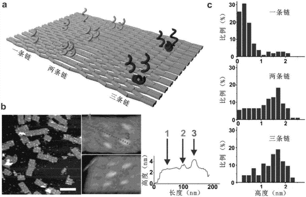
[0041] Example 2: Effect of defect size of "eight-dot" defect pattern on DNA origami (that is, each "dot" defect contains different number of DNA single strands) on its effect of copper metallization.

[0042] We designed such an array on the square DNA origami, respectively stretching out one, two and three 15bp DNA single strands ( figure 2 ), in view of the resolution of the square DNA origami in the long axis direction, when there are two or three DNA strands at each point, the horizontal spacing between two adjacent single strands protruding out is about 5.4nm, and the vertical spacing is about 3nm, so The straight-line distance between two adjacent single strands will be shortened to about 6nm. We were expecting to see significantly different metallization results for one single-strand defect versus multiple single-strands. The results were as we expected. After the metallization of the sample, it was obvious that the sites with only one 15bp DNA single strand per poin...

Embodiment 3

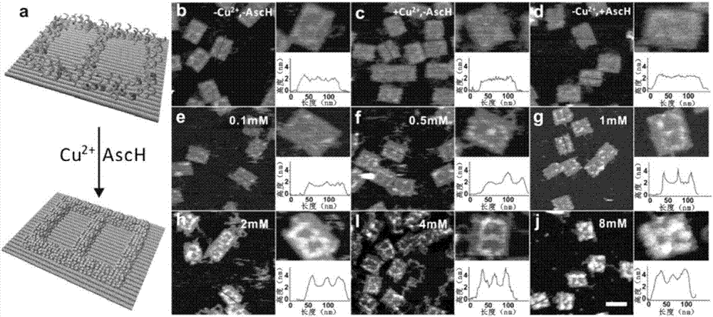
[0043] Example 3: Effects of different concentrations of copper ions on the metallization effect in the metallization reaction solution

[0044] We further investigated CuCl 2 Concentration effect on defect copper metallization on DNA origami, we keep the rest of the reaction conditions unchanged and only gradually change the CuCl 2 concentration. Here, instead of using the DNA origami with the defect pattern of "seven points", the defect pattern of "number 8" is introduced into the square DNA origami. The concentration of copper ions in the added metallization reaction solution varies from 0.1 mM to 8 mM. When the concentration of copper ions is relatively low (0.1mM), from the attached image 3 In the AFM image in e, it can be seen that only sporadic brighter points appear. As the concentration of copper chloride increases, the lines of the pattern become more and more continuous. When it reaches 2mM, the complete number 8 is more obvious. Manifested on DNA origami. The...


PUM

PropertyMeasurementUnit
heightaaaaaaaaaa

Abstract

The invention provides a manufacture method of metal nano circuit patterns based on DNA nano structures. The method includes taking DNA paper folding structures fixed to surfaces as templates, introducing artificial defects onto the templates, and performing selective metallization on the templates with the artificial defects so as to create the metal nano circuit patterns based on the DNA nano structures. The manufacture method is simple, rapid and effective, and a series of metal nano patterns with only few nanometers of zero-dimensional, one-dimensional and two-dimensional line width can be acquired through accurate positioning of DNA paper folding. DNA paper folding mainly applied to the manufacture method has high biocompatibility, and other needed chemical and biological materials do not have toxicity on human bodies; a novel thought and a novel technical support are provided for creating a nano circuit by 'bottom-to-up' self-assembly and breaking through the limit of conventional photolithography.

Description

technical field [0001] The invention relates to the field of nano-manufacturing, in particular to a method for preparing a metal nano-circuit pattern based on a DNA nano-structure. Background technique [0002] Integrated Circuit (IC for short) is a new type of semiconductor device developed in the early 1960s. In electronics, integrated circuit technology is actually a circuit miniaturization technology. It is a semiconductor manufacturing process such as oxidation, photolithography, diffusion, epitaxy, and aluminum evaporation. Components such as capacitors and capacitors and the connecting wires between them are all integrated on a small piece of silicon, and then soldered to the electronic devices packaged in a tube. At present, information technology characterized by digitalization and networking is infiltrating and transforming various industries and trades, profoundly changing human production and lifestyle as well as economic, social, political, and cultural fields....

Claims


Application Information

Patent Timeline
Patent Type & Authority Applications(China)
IPC IPC(8): B82B3/00B82Y40/00
CPCB82B3/0019B82Y40/00
Inventor 樊春海柳华杰贾思思王建榜
Owner SHANGHAI INST OF APPLIED PHYSICS - CHINESE ACAD OF SCI
Why Eureka
Try Eureka