Super-hydrophobic surface reinforced Raman substrate prepared from silicon nanometer dielectric material and preparation method thereof

A technology of super-hydrophobic surface and Raman substrate, which is applied in nanotechnology, Raman scattering, nanotechnology, etc. for materials and surface science, and can solve the problem of mild reaction conditions, time-consuming and high cost, and unfavorable practical utilization, etc. problem, to achieve the effect of simple method, low cost, and changing the local distribution of the light field

Active Publication Date: 2017-08-18
SUN YAT SEN UNIV
View PDF7 Cites 5 Cited by
  • Summary
  • Abstract
  • Description
  • Claims
  • Application Information

AI Technical Summary

Problems solved by technology

However, the preparation of the superhydrophobic substrate involves complex processes and requires special processing equipment such as photolithography and ion beam etching, which is not conducive to practical application.
In addition, this method is time-consuming and costly. Although the surface morphology of the obtained substrate can be well controlled, the reaction conditions are not mild and there are many process steps.
[0006] Therefore, low-cost, easy-to-prepare, high-sensitivity SERS substrates that can be used for trace tracking detection still need to be explored.

Method used


Image

  • Super-hydrophobic surface reinforced Raman substrate prepared from silicon nanometer dielectric material and preparation method thereof
  • Super-hydrophobic surface reinforced Raman substrate prepared from silicon nanometer dielectric material and preparation method thereof
  • Super-hydrophobic surface reinforced Raman substrate prepared from silicon nanometer dielectric material and preparation method thereof

Examples


Embodiment 1

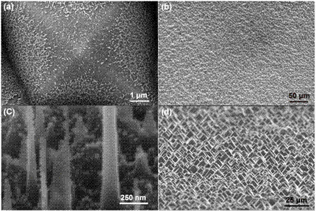
[0040] 1) Use n-type double-sided polished silicon wafers, cut into 2×2 cm 2 size, put them in acetone solution and alcohol solution and ultrasonically clean them for 15 min respectively;

[0041] 2) Then rinse the residual alcohol solution on the surface of the silicon wafer with deionized water, and ultrasonically clean it in deionized water for 15 minutes, then immerse the silicon wafer in a beaker filled with hydrogen peroxide and concentrated sulfuric acid and heat at 80 °C for 30 minutes to remove the residual alcohol solution on the surface. Organic pollutants, the volume ratio of the solution H 2 SO 4 :H 2 o 2 =3:1, finally take out the silicon wafer and dry it with a large amount of deionized nitrogen;

[0042] 3) Place the cleaned silicon wafer in a NaOH solution with a mass fraction of 20% and heat it in a water bath at 80 °C for 2 min, then quickly take it out and rinse it in deionized water;

[0043] 4) Then place the silicon wafer in a mixed solution of eth...


PUM

PropertyMeasurementUnit
widthaaaaaaaaaa
heightaaaaaaaaaa
lengthaaaaaaaaaa

Abstract

The invention relates to a super-hydrophobic surface reinforced Raman substrate prepared from a silicon nanometer dielectric material and a preparation method thereof. The substrate is formed by a silicon micron cone integrated with metal nanoparticles and a cascade structure formed by nanowires. The preparation method of the structure comprises the following steps that S1, a silicon wafer is put into a micromolecule alcohol and strong base mixed solution; the silicon micron cone structure is built through water bath heating; S2, the silicon micron cone structure is put into mixed corrosion liquid of silver salt solution and HF solution; etching is performed to obtain a silicon micron/nanometer cascade structure; S3, the silicon micron/nanometer cascade structure obtained in the S2 is soaked by acid solution so as to remove silver nanoparticles remained at the surface; then, the silicon micron/nanometer cascade structure is subjected to gold nanoparticle wrapping covering; S4, low-surface-energy substances are used for performing surface covering modification on the gold-silicon composite structure obtained in the S3, i.e., the super-hydrophobic surface reinforced Raman substrate is obtained. The super-hydrophobic surface reinforced Raman substrate provided by the invention has super-hydrophobic property; the static contact angle with water is 160 to 162 degrees.

Description

technical field [0001] The invention relates to the field of molecular detection, in particular to a super-hydrophobic surface-enhanced Raman substrate prepared by using a silicon nano-dielectric material and a preparation method thereof. Background technique [0002] Surface enhanced Raman scattering (SERS) is due to the field enhancement effect caused by the metal surface plasmon resonance, which results in an enhanced Raman scattering signal of molecules adsorbed on the surface of the metal nanostructure. This electromagnetic field-enhancing effect results from the localized effect of the light field, usually confined to an extremely small area, often referred to as a "hot spot". Because of its incomparable signal enhancement effect of ordinary Raman, SERS can even realize single-molecule detection. As a new type of highly sensitive detection method, SERS has been widely used in the fields of spectral analysis, biological detection and imaging. [0003] For the applicati...

Claims


Application Information

Patent Timeline
Patent Type & Authority Applications(China)
IPC IPC(8): G01N21/65B82Y30/00B82Y40/00
CPCG01N21/658B82Y30/00B82Y40/00
Inventor 陈焕君陈学贤邓少芝许宁生
Owner SUN YAT SEN UNIV
Why Eureka
Try Eureka