Chalcogenide optical element with electromagnetic shielding performance and preparation method thereof

A technology for optical components and electromagnetic shielding, applied in optical components, optics, instruments, etc., can solve the problems of increasing the technical difficulty of chalcogenide glass windows and optical components, damage to the optical surface of chalcogenide glass, and difficult process control, etc., to achieve electromagnetic Good shielding performance, increased infrared light transmittance, strong electromagnetic shielding effect

Active Publication Date: 2017-09-08
CHINA BUILDING MATERIALS ACAD
View PDF8 Cites 4 Cited by
  • Summary
  • Abstract
  • Description
  • Claims
  • Application Information

AI Technical Summary

Problems solved by technology

Metal grid infrared electromagnetic shielding film has been used in ZnS, sapphire, AlON and MgF 2 Many infrared windows and optical devices have been applied in practice, but they still have defects such as complex preparation process, difficult process control, poor mechanical properties, low light flux and moiré interference fringes.
At the same time, chalcogenide glass itself is a soft and brittle material with low surface hardness and relatively weak mechanical strength.
Therefore, steps such as "high-speed spin coating", "laser direct writing etching mask", "vacuum coating" and "organic solvent deglue" in the production process of the metal grid are likely to cause damage to the optical surface of the chalcogenide glass. damage, which greatly increases the technical difficulty of chalcogenide glass windows and optical components to achieve electromagnetic shielding functions

Method used


Image

  • Chalcogenide optical element with electromagnetic shielding performance and preparation method thereof

Examples


preparation example Construction

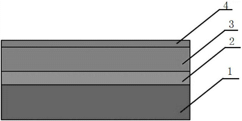
[0032] One embodiment of the present invention proposes a method for preparing a chalcogenide optical element with electromagnetic shielding properties, comprising the following steps:

[0033] (1) Coating an inorganic film layer on the surface of the base layer of the chalcogenide optical element;

[0034] Preferably, the coating method of the inorganic film layer described in the embodiments of the present invention is electron beam evaporation or radio frequency magnetron sputtering; the coating step of the inorganic film layer includes: the background vacuum degree is less than 8× 10 -4 Pa, turn on the baking lamp before coating, heat the surface of the base layer of the chalcogenide glass coating to 50-100°C and keep it warm for 20-30min, turn on the ion source and use Ar + Ions clean the surface of the chalcogenide optical element for 15-20 minutes. After cleaning, turn on the electron gun to vapor-deposit the material of the inorganic film layer on the surface of the b...

Embodiment 1

[0059] Use ethanol-ether mixture and absolute ethanol to wipe the surface of the base layer of the flat chalcogenide optical element to the cleanliness of the coating; use the electron beam evaporation method for coating, and the background vacuum is 5×10 -4 Pa, turn on the baking lamp before coating, heat the surface of the plated chalcogenide glass window to 80°C and keep it warm for 20min, turn on the ion source and use Ar + Ion-cleaned the surface of the plated parts for 15 minutes, and finally turned on the electron gun to clean the high-purity SiO 2 The film material is evaporated to prepare SiO 2 The thickness of the film layer is 15nm; mix the silicone resin and the curing agent in a volume ratio of 30:1, stir well for 2 minutes, and mix in 5×10 -2 The vacuum degree of Pa was discharged for 15 minutes to obtain the organic colloid, and the obtained organic colloid was uniformly sprayed on the SiO 2 On the surface of the film, an organic coating is formed after it is ...

Embodiment 2

[0062] Use ethanol-ether mixture and absolute ethanol to wipe the surface of the base layer of the flat chalcogenide optical element to the cleanliness of the coating; use the radio frequency magnetron sputtering method for coating, and the background vacuum is 4×10 -4 Pa, turn on the baking lamp before coating, heat the surface of the plated chalcogenide glass window to 50°C and keep it warm for 30min, turn on the ion source and use Ar + Ions were used to ion-clean the surface of the plated part for 20 minutes, and finally the electron gun was turned on to clean the surface of the high-purity Al 2 o 3 The film material is evaporated to prepare Al 2 o 3 The thickness of the film layer is 10nm; mix the polyimide resin and the curing agent in a volume ratio of 25:1, stir well for 2min, and mix in 5×10 - 2 Under the vacuum degree of Pa, debubble 15min, obtain organic colloid, utilize the organic colloid that the organic colloid that obtains is evenly sprayed on Al 2 o 3 On ...


PUM

PropertyMeasurementUnit
thicknessaaaaaaaaaa
thicknessaaaaaaaaaa
thicknessaaaaaaaaaa

Abstract

The invention relates to a chalcogenide optical element with an electromagnetic shielding performance and a preparation method thereof. The method includes following steps: (1) plating an inorganic membrane layer on the surface of a substrate of the chalcogenide optical element; (2) spraying an organic coating on the surface of the inorganic membrane layer; and (3) transferring a graphene infrared transmitting electromagnetic shielding film to the surface of the organic coating to obtain the chalcogenide optical element with the electromagnetic shielding performance. According to the chalcogenide optical element with the electromagnetic shielding performance, compared with the optical element regarding a metal mesh as a shielding body, the realization performance is great, the manufacturing method is simple, and the manufacturing cost is low; according to the chalcogenide optical element with the electromagnetic shielding performance, the light absorption coefficient in the work waveband of 1.06-12 [mu]m is small, the light transmittance is high, and the electromagnetic shielding effect is high; and the sheet resistance is lower than 35 ohms per square, the electromagnetic shielding efficiency is greater than 15 dB, and the infrared transmission loss is less than 3%.

Description

technical field [0001] The invention relates to a chalcogenide optical element, in particular to a chalcogenide optical element with electromagnetic shielding performance and a preparation method thereof. Background technique [0002] Chalcogenide glass is a kind of infrared transparent material with excellent performance. It has high transmittance and extremely low temperature thermal coefficient of refraction index in the three main infrared atmospheric windows of 1.06 μm, 3-5 μm and 8-12 μm. In recent years, with the popularity of passive athermal design in infrared optical systems, chalcogenide glass windows and optical components have shown high application value and broad application prospects in various infrared imaging, guidance, and detection systems. [0003] In practical applications, especially in the infrared optical systems of various military weapons, in order to avoid the interference of the harsh electromagnetic environment on the equipment, it is usually ne...

Claims


Application Information

Patent Timeline
Patent Type & Authority Applications(China)
IPC IPC(8): G02B1/113G02B1/111G02B1/10G02B1/00
CPCG02B1/00G02B1/10G02B1/111G02B1/113
Inventor 邱阳陈玮金扬利祖成奎韩滨徐博
Owner CHINA BUILDING MATERIALS ACAD
Why Eureka
Try Eureka