Nanometer layered metal compound electrode material grown on conductive substrate and preparation and application of nanometer layered metal compound electrode material

A metal compound, conductive substrate technology, applied in the field of electrochemical materials, can solve the problems of difficult to achieve large-scale preparation of nano-material products, complex preparation process conditions, high equipment conditions, etc., to achieve excellent electrochemical performance, controllable line height , The effect of process environmental protection

Inactive Publication Date: 2017-09-08
SOUTH CHINA UNIV OF TECH
View PDF4 Cites 8 Cited by
  • Summary
  • Abstract
  • Description
  • Claims
  • Application Information

AI Technical Summary

Problems solved by technology

[0004] At present, researchers have invented a variety of synthesis strategies and technologies for transition metal nanosheet materials, but these methods usually have high requirements on equipment conditions, and need to add various chemicals such as hexamethylenetetramine or urea, causing environmental pollution. Pollution
Complex preparation process conditions and high costs make it difficult to realize the macro preparation of this type of nanomaterial products

Method used


Image

  • Nanometer layered metal compound electrode material grown on conductive substrate and preparation and application of nanometer layered metal compound electrode material
  • Nanometer layered metal compound electrode material grown on conductive substrate and preparation and application of nanometer layered metal compound electrode material
  • Nanometer layered metal compound electrode material grown on conductive substrate and preparation and application of nanometer layered metal compound electrode material

Examples


Embodiment 1

[0036] A preparation method for growing a nano-layered metal compound electrode material on a conductive substrate, comprising the following steps:

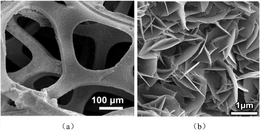
[0037] (1) Cut the nickel foam into 4cm×2cm, soak it in alcohol and acetone ultrasonically for 30min in turn, wash it with deionized water, and dry it at 60°C for later use;

[0038] (2) Prepare 1mmol / L CoCl with cobalt chloride and water 2 Precursor solution, stirred for 30 minutes to make the precursor solution evenly mixed;

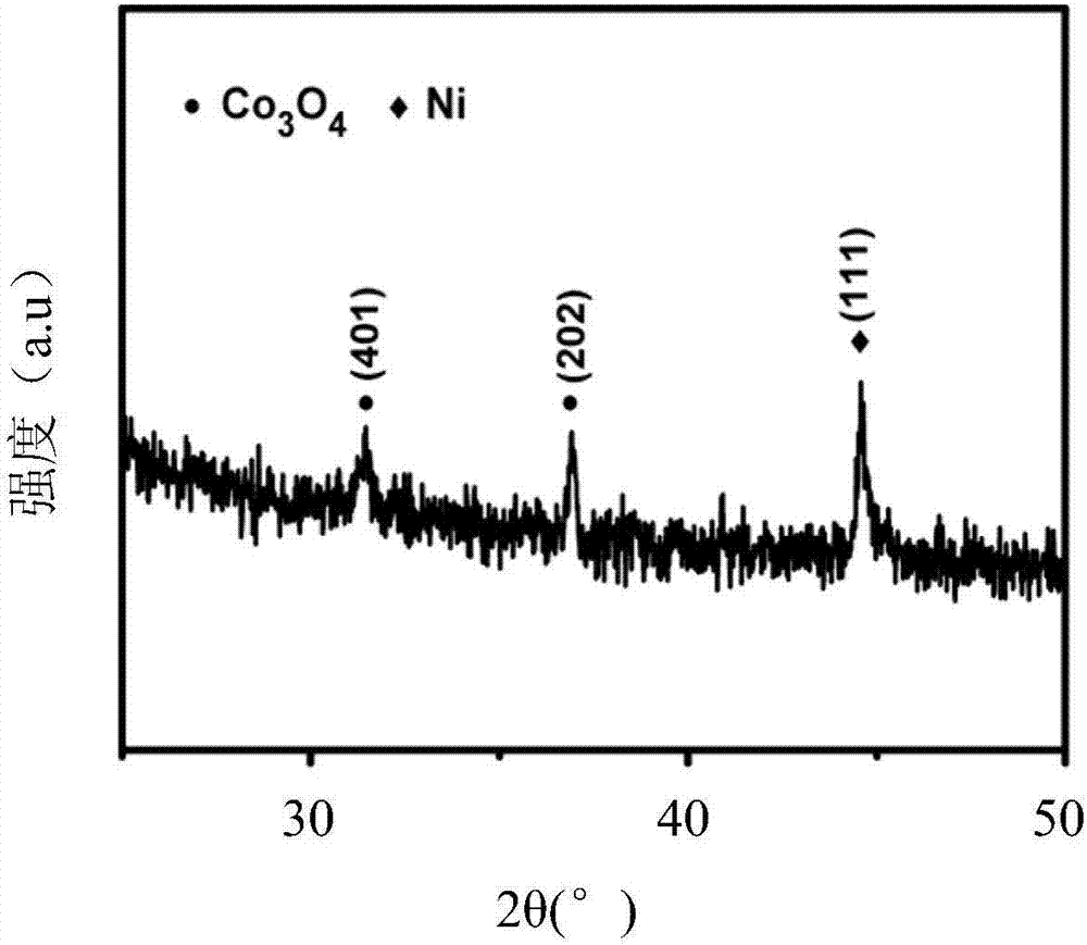
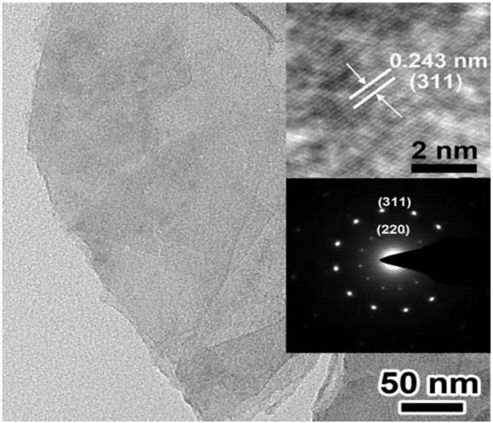
[0039] (3) Fill the above-mentioned precursor solution of about 80% volume in the reaction kettle liner of polytetrafluoroethylene material; Then place the foamed nickel through pretreatment in the reaction kettle liner, then seal with a stainless steel reaction kettle, Hydrothermal reaction at 100°C for 10 hours. After the reaction is completed, the hydrothermal kettle is naturally cooled, and the nickel foam is taken out, washed several times with ethanol and deionized water, and dried at 60°C for 12 h...

Embodiment 2

[0045] A preparation method for growing a nano-layered metal compound electrode material on a conductive substrate, comprising the following steps:

[0046] (1) Cut the nickel foil into 4cm×2cm, soak it in alcohol and acetone ultrasonically for 30 minutes, wash it with deionized water, and dry it at 80°C for later use;

[0047] (2) Prepare 1mmol / L NiCl with nickel chloride and water 2 Precursor solution, stirred for 30 minutes to make the precursor solution evenly mixed;

[0048] (3) Fill the above-mentioned precursor solution of about 90% volume in the reaction kettle liner of polytetrafluoroethylene material; Then place the pretreated nickel foil in the reaction kettle liner, and then seal it with a stainless steel reaction kettle, Hydrothermal reaction at 100°C for 10 hours, after the reaction was completed, the hydrothermal kettle was cooled naturally, the nickel foil was taken out, washed several times with ethanol and deionized water, and dried at 100°C for 6 hours to obt...

Embodiment 3

[0052] A preparation method for growing a nano-layered metal compound electrode material on a conductive substrate, comprising the following steps:

[0053] (1) Cut the nickel foam into 4cm×2cm, soak it in alcohol and acetone ultrasonically for 30 minutes, wash it with deionized water, and dry it at 100°C for later use;

[0054] (2) Prepare 1mmol / L MnCl with manganese chloride and water 2 Precursor solution, stirred for 30 minutes to make the precursor solution evenly mixed;

[0055] (3) Fill the above-mentioned precursor solution of about 50% volume in the reaction kettle liner of polytetrafluoroethylene material; Then place the foamed nickel through pretreatment in the reaction kettle liner, then seal with a stainless steel reaction kettle, Put it in 80°C hydrothermal reaction for 20 hours, after the reaction is completed, the hydrothermal kettle is naturally cooled, take out the foamed nickel, wash it with ethanol and deionized water several times, and dry it at 60°C for 1...


PUM


Abstract

The invention belongs to the technical field of an electrochemical material, and discloses a nanometer layered metal compound electrode material grown on a conductive substrate and preparation and application of the nanometer layered metal compound electrode material. The method comprises the steps of (1) pre-processing the conductive substrate for use; (2) preparing a precursor solution from a divalent transition metal salt with water; and (3) placing the precursor solution and the pre-processed conductive substrate in a hydrothermal reaction kettle for sealing, performing hydrothermal reaction for 8-20 hours at 80-200 DEG C, and performing cooling, washing and drying to obtain the nanometer layered metal compound electrode material grown on the conductive substrate. The method has the advantages that a pH value is not needed to be adjusted, an organic surfactant is not needed to be added, and the process is environmental-friendly; and a metal compound in the prepared material is high in crystallinity and uniform in morphology size, the material is directly grown on a metal nickel conductive substrate, the obtained material has excellent electrochemical performance and can be widely applied to an electrochemical energy storage device electrode material.

Description

technical field [0001] The invention belongs to the technical field of electrochemical materials, and relates to a nano-layer structure metal compound electrode material grown on a conductive substrate and its preparation method and application. Compound hydroxide\oxide. Background technique [0002] With the rapid growth of the global population and the rapid development of the social economy, the traditional fossil fuel resources are gradually exhausted, and the problem of environmental pollution is becoming more and more serious. Therefore, the development of new energy and new energy materials has become an important strategic choice for the sustainable development of society, including solar energy, wind energy, water energy, biomass energy, geothermal energy and hydrogen energy. In order to fully develop and utilize these new energy sources, it is urgent to develop matching high-performance electrochemical energy storage and conversion technologies, as well as corresp...

Claims


Application Information

Patent Timeline
IPC IPC(8): H01G11/30H01G11/86H01M4/139H01M4/36
CPCH01G11/30H01G11/86H01M4/139H01M4/366Y02E60/10
Inventor 侯冬曼周凯周伟家
Owner SOUTH CHINA UNIV OF TECH
Why Eureka
Try Eureka