Check patentability & draft patents in minutes with Patsnap Eureka AI!

Array substrate and display device

An array substrate and substrate technology, applied in semiconductor devices, electrical components, circuits, etc., can solve the problems of high cost, limited resources, poor mechanical stability, etc., and achieve the effect of reducing potential harm

Active Publication Date: 2019-12-31
TCL CHINA STAR OPTOELECTRONICS TECH CO LTD
View PDF4 Cites 0 Cited by
  • Summary
  • Abstract
  • Description
  • Claims
  • Application Information

AI Technical Summary

Problems solved by technology

These heavy metal materials are limited in resources, high in cost, and have certain environmental pollution hazards. Therefore, it is the future development trend to reduce or even eliminate metal elements in display devices.
For example, ITO (Indium tin oxide, indium tin oxide) electrodes have poor mechanical stability, and the increasing shortage of indium resources leads to continuous increase in its cost, and also brings metal environmental problems, so some alternative environmentally friendly electrode materials are urgently needed
[0003] In addition, as the size of traditional silicon semiconductor devices continues to shrink, some unavoidable constraints continue to emerge, such as short channel effects, statistical fluctuations in doping concentration at small sizes, resulting in non-uniform device properties

Method used


Image

  • Array substrate and display device
  • Array substrate and display device
  • Array substrate and display device

Examples


Embodiment Construction

[0036] The implementation of the present invention will be described in detail below in conjunction with the accompanying drawings and examples, so as to fully understand and implement the process of how to apply technical means to solve technical problems and achieve technical effects in the present invention. It should be noted that, as long as there is no conflict, each embodiment and each feature in each embodiment of the present invention can be combined with each other, and the formed technical solutions are all within the protection scope of the present invention.

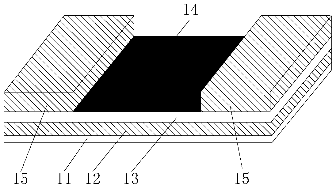
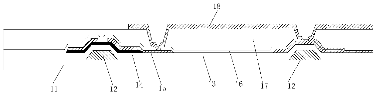
[0037] Carbon is currently one of the materials with the most abundant nanostructures and characteristics, such as fullerenes, carbon quantum dots, carbon nanotubes, graphene, etc., which have attracted the attention of researchers due to their excellent chemical, physical, mechanical and electronic properties. Great research interests and experimental applications. Combining the unique properties of dimensi...


PUM


Abstract

The invention provides an array substrate and a display device, including a thin film transistor, and the thin film transistor includes: a first conductive layer disposed on a substrate; an insulating layer disposed on the first conductive layer and a bare substrate; an active layer, which is arranged on the insulating layer; the second conductive layer, which is arranged on the active layer; the passivation layer, which is arranged on the second conductive layer and the exposed insulating layer, wherein the first conductive layer, the active layer and the second conductive layer are made of transparent and conductive carbon compound material. The invention can construct green and cheap devices, and reduce the potential harm of metal elements to the environment and human body.

Description

technical field [0001] The present invention belongs to the field of display technology, and in particular, relates to an array substrate and a display device. Background technique [0002] Currently used liquid crystal display devices or organic light emitting diode display devices contain expensive heavy metals such as indium, copper, molybdenum, and tin. These heavy metal materials have limited resources, high cost, and certain environmental pollution hazards. Therefore, reducing or even eliminating metal elements in display devices is a future development trend. For example, ITO (Indium tin oxide, indium tin oxide) electrodes have poor mechanical stability, and the increasing shortage of indium resources leads to continuous increase in its cost, and also brings metal environmental problems, so some alternative environmentally friendly electrode materials are urgently needed. [0003] In addition, as the size of traditional silicon semiconductor devices continues to shri...

Claims


Application Information

Patent Timeline
IPC IPC(8): H01L27/32H01L51/52
CPCH10K59/123H10K59/12H10K50/80H10K50/805H10K59/10
Inventor 谢华飞
Owner TCL CHINA STAR OPTOELECTRONICS TECH CO LTD
Features
  • R&D
  • Intellectual Property
  • Life Sciences
  • Materials
  • Tech Scout
  • Unparalleled Data Quality
  • Higher Quality Content
  • 60% Fewer Hallucinations
Learn More