Light-emitting diode epitaxial wafer and manufacturing method thereof

A technology for light-emitting diodes and a manufacturing method, which is applied to electrical components, circuits, semiconductor devices, etc., can solve the problems of unclear well-barrier interface and low crystal quality of quantum wells, and achieves good thermal conductivity, saving process flow, and thermal stability. good effect

Inactive Publication Date: 2017-09-08
XIANGNENG HUALEI OPTOELECTRONICS
View PDF3 Cites 7 Cited by
  • Summary
  • Abstract
  • Description
  • Claims
  • Application Information

AI Technical Summary

Problems solved by technology

[0013] In view of this, the present invention provides an epitaxial wafer of a light-emitting diode and a manufacturing method there...

Method used


Image

  • Light-emitting diode epitaxial wafer and manufacturing method thereof
  • Light-emitting diode epitaxial wafer and manufacturing method thereof
  • Light-emitting diode epitaxial wafer and manufacturing method thereof

Examples


Embodiment 1

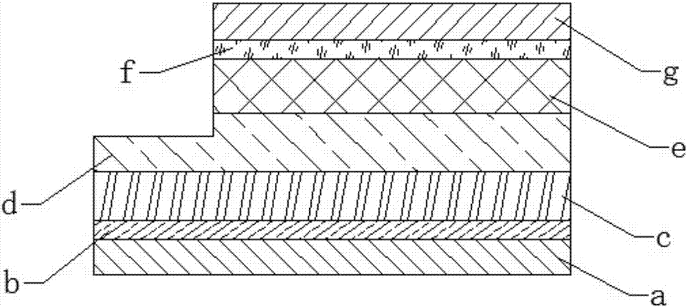
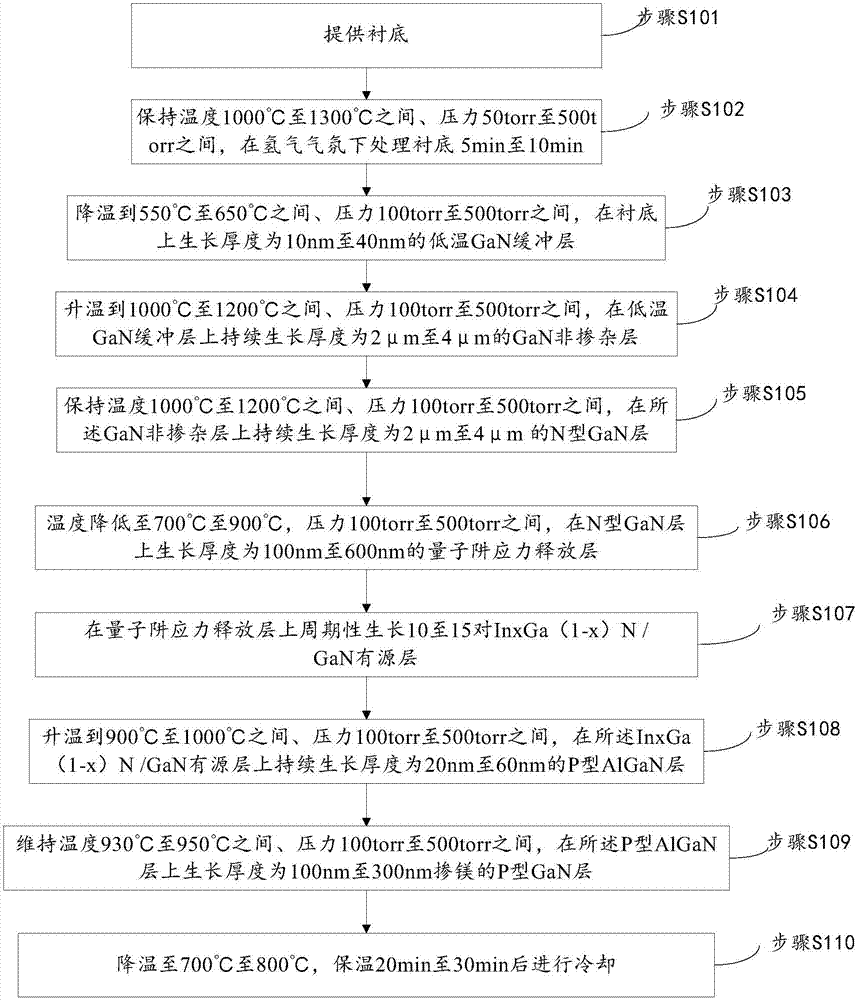
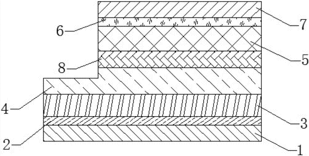
[0065] refer to figure 2 and image 3 , the present embodiment provides a method for manufacturing a light-emitting diode epitaxial wafer, comprising:

[0066] Step S101, providing a substrate 1;

[0067] Step S102, keeping the temperature between 1000° C. and 1300° C. and the pressure between 50 torr and 500 torr, and treating the substrate in a hydrogen atmosphere for 5 minutes to 10 minutes;

[0068] Step S103, lower the temperature to 550°C to 650°C, and the pressure to 100torr to 500torr, and grow a low-temperature GaN (gallium nitride) buffer layer 2 with a thickness of 10nm to 40nm on the substrate 1;

[0069] Step S104, raising the temperature to between 1000°C and 1200°C and the pressure between 100torr and 500torr, and continuously growing a GaN non-doped layer 3 with a thickness of 2 μm to 4 μm on the low-temperature GaN buffer layer 2;

[0070] Step S105, keeping the temperature between 1000° C. and 1200° C. and the pressure between 100 torr and 500 torr, and c...

Embodiment approach

[0081] As a preferred embodiment, the In x Ga (1-x) The In doping concentration of the N (x=0.015-0.25) well layer is 1E+20-5E+20.

[0082] As a preferred implementation manner, the magnesium doping concentration of the P-type AlGaN layer 6 is 5E+18-1E+19, and the Al doping concentration is 1E+20-3E+20.

[0083] As a preferred implementation manner, the Mg doping concentration of the P-type GaN layer 7 is 1E+19-1E+20.

[0084] The manufacturing method of the light-emitting diode epitaxial wafer provided by this embodiment can effectively improve the crystallization quality of the quantum well by adding the quantum well stress release layer, so that the interface between the well layer and the barrier layer of the quantum well is clearer and steeper, and the quantum well is more sensitive to electrons. and hole binding, thereby improving the luminous efficiency of the LED chip.

Embodiment 2

[0086] refer to image 3 , the present embodiment provides a method for fabricating an epitaxial wafer of a light emitting diode, comprising:

[0087] Step S201, providing a substrate 1;

[0088] Preferably, the substrate 1 is a sapphire substrate;

[0089] Step S202, maintaining the temperature at 1100° C., maintaining the pressure in the reaction chamber at 500 torr, and processing the substrate in a hydrogen atmosphere for 6 minutes;

[0090] Step S203, lowering the temperature to 550° C., maintaining the pressure of the reaction chamber at 500 torr, and growing a low-temperature GaN buffer layer 2 with a thickness of 20 nm on the substrate 1;

[0091] In step S204, the temperature is raised to 1100° C., the pressure of the reaction chamber is maintained at 200 torr, and a GaN non-doped layer 3 with a thickness of 3 μm is continuously grown on the low-temperature buffer layer 2 ;

[0092] Step S205, maintaining the temperature at 1100° C., maintaining the pressure of the...


PUM

PropertyMeasurementUnit
Thicknessaaaaaaaaaa
Thicknessaaaaaaaaaa
Thicknessaaaaaaaaaa

Abstract

The invention discloses a light-emitting diode epitaxial wafer and a manufacturing method thereof. The epitaxial wafer comprises a substrate, a low-temperature GaN buffer layer formed on the substrate, a GaN non-doped layer formed on the low-temperature GaN buffer layer, an N-type GaN layer formed on the GaN non-doped layer, a quantum well stress release layer formed on the N-type GaN layer, an InxGa(1-x)N/GaN active layer formed on the quantum well stress release layer, a P-type AlGaN layer formed on the InxGa(1-x)N/GaN active layer, and a P-type GaN layer formed on the P-type AlGaN layer; through the quantum well stress release layer, the crystal quality of a quantum well can be effectively improved, so that the trap layer and barrier layer interface of the quantum well is more clear and abrupt, the binding effect of the quantum well for electrons and holes is improved, and the luminous efficiency of an LED chip is improved.

Description

technical field [0001] The invention relates to the technical field of semiconductors, in particular to an epitaxial wafer of a light emitting diode and a manufacturing method thereof. Background technique [0002] In recent years, the research on InGaN / GaN multiple quantum wells (MQW) as the active region of blue-green and near-ultraviolet light-emitting diodes has become more and more extensive and in-depth. People have improved the luminescence characteristics of InGaN / GaN quantum wells by optimizing the growth temperature of quantum wells, the doping of barrier layers, the thickness of wells and barriers, etc. Due to their excellent electrochemical properties, GaN-based materials have been widely used in the field of microelectronics and optoelectronics. Wide range of applications. However, with the needs of social development, people have higher and higher requirements for the brightness of GaN-based light-emitting diodes. [0003] refer to figure 1 , the existing st...

Claims


Application Information

Patent Timeline
IPC IPC(8): H01L33/00H01L33/04H01L33/12
CPCH01L33/007H01L33/04H01L33/12
Inventor 徐平
Owner XIANGNENG HUALEI OPTOELECTRONICS
Why Eureka
Try Eureka