Flip LED chip array structure and preparation method thereof

A technology of LED chip and array structure, applied in electrical components, circuits, semiconductor devices, etc., can solve the problems of high current density, increased number of chip cutting, small chip power, etc., to achieve uniform current density distribution and effective light emitting area. Improve, fit the effect of increasing the effective area

Pending Publication Date: 2017-09-08
苏州瑞而美光电科技有限公司
View PDF4 Cites 15 Cited by
  • Summary
  • Abstract
  • Description
  • Claims
  • Application Information

AI Technical Summary

Problems solved by technology

The traditional method has the following disadvantages: (1) Each chip must be individually packaged into a small tube socket and then pasted on a large heat dissipation module. The power of a single chip is not large, and the process is cumbersome; The electrodes are all above the active area, which has a light-absorbing effect on the light emitted by the active area, and there will be more than 20%-30% light loss, and the light output efficiency is low; (3) The front-mounted chip conducts heat through metal leads, and the effective area of ​​heat conduction is small. The heat conduction path is long, and the heat dissipation effect is not as good as that of the flip chip
[0003] Although there are currently LED chip flip-chip solutions, the traditional LED chip flip-chip solutions have the following disadvantages: (1) The current distribution of flip-chip LED chips is uneven, and the flip-chip electrodes are single, and only one P-type electrode corresponds to one N-type electrode. The current density in the local area of ​​the chip is too high, and the uneven current directly causes the power of the chip to be limited. Under the high current working environment, the service life of the chip is shortened; (2) Due to the power limit, the size of the LED chip is also limited. , so that the effective contact area between the P-type electrode of the chip and the heat dissipation substrate is also reduced, and the heat dissipation effect is limited. On the same heat-dissipating substrate, the cumbersomeness of the flip-chip welding process is increased; (4) The limitation of the chip size leads to an increase in the number of cutting of the same epitaxial wafer chip, and the loss caused by cutting directly affects the effective utilization of the product

Method used


Image

  • Flip LED chip array structure and preparation method thereof
  • Flip LED chip array structure and preparation method thereof
  • Flip LED chip array structure and preparation method thereof

Examples


Embodiment

[0045] Such as figure 1 As shown, the preparation method of the flip-chip LED chip array structure includes the following steps:

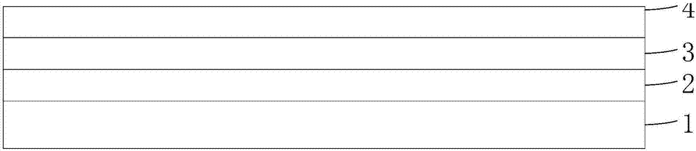
[0046] (1) A multi-element composite of one or more materials among sapphire, gallium nitride, and aluminum nitride is selected as the transparent substrate 1 for epitaxial growth.

[0047] (2) On the surface of the transparent substrate 1, the buffer layer 2, the N-type GaN semiconductor structure layer 3 and the P-type GaN semiconductor structure layer 4 are epitaxially grown in sequence to obtain a substrate epitaxial wafer, such as figure 2 shown.

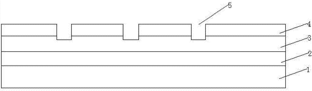
[0048] (3) A plurality of N-type region windows 5 are etched on the surface of the epitaxial structure layer by using semiconductor process technologies such as photolithography, development, and etching, and a plurality of small-area N-type region windows 5 are arranged in an array, such as image 3 shown.

[0049] (4) The current diffusion layer 6 is prepared by photolithographic masking, sput...


PUM


Abstract

The invention discloses a flip LED chip array structure. The flip LED chip array structure comprises a transparent substrate made of a transparent material; a buffer layer arranged on one surface of the transparent substrate; an N-type semiconductor structural layer and a P-type semiconductor structural layer formed on the buffer layer; a current diffusion layer made of a conductive material; a passivation layer arranged above the P-type semiconductor structural layer, made of a transparent insulating material, and covering the current diffusion layer, the P-type semiconductor structural layer, and the N-type semiconductor structural layer; a plurality of N-type electrode window regions arranged in an array manner and contacted with the N-type semiconductor structural layer; and P-type electrode window regions contacted with the P-type semiconductor structural layer. The N-type electrode window regions are provided with N-type electrodes, the P-type electrode window regions are provided with P-type electrodes, and the heights of the P-type electrodes and the N-type electrodes are the same. According to the flip LED chip array structure, the effective light-emitting area of the high-power LED chip is increased, the effective contact area between the chip electrodes and the heat radiation substrate is increased, the heat radiation effect is better, and the service lifetime of the chip is prolonged.

Description

technical field [0001] The invention relates to a flip-chip LED chip, in particular to a flip-chip LED chip array structure and a preparation method thereof. Background technique [0002] As the fourth-generation green lighting source, white LED light source is expected to replace traditional lighting sources such as incandescent lamps, fluorescent lamps, and halogen lamps because of its advantages such as high efficiency, high brightness, small size, long service life, low power consumption, and environmental protection. , is a new generation of widely used high-quality light source, and will become an indispensable lighting tool for industry and life. However, at present, it is necessary to increase the power of the LED chip, and to better solve the heat dissipation capacity of the chip and improve the brightness of the chip, which is the biggest technical bottleneck encountered by high-power LEDs at present. The traditional LED packaging method adopts the formal packagin...

Claims


Application Information

Patent Timeline
IPC IPC(8): H01L33/52H01L33/64H01L33/38H01L33/12H01L33/14
CPCH01L33/12H01L33/14H01L33/38H01L33/52H01L33/64
Inventor 王峰
Owner 苏州瑞而美光电科技有限公司
Why Eureka
Try Eureka