Ink-jet printing based conductive circuit printing process
A conductive circuit and inkjet printing technology, which is applied in printed circuit, printed circuit manufacturing, conductive pattern formation, etc., can solve the problems of narrow selection of printing substrates, poor conductivity of printed circuits, poor connection between conductive layer and substrate, etc. Achieve excellent mechanical properties, good insulation, and improved bonding force
- Summary
- Abstract
- Description
- Claims
- Application Information
AI Technical Summary
Problems solved by technology
Method used
Image

Examples
Embodiment 1
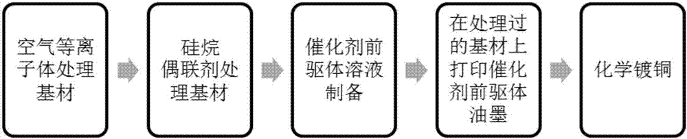
[0032] A conductive circuit printing process based on inkjet printing, comprising the following steps:
[0033] (1) Substrate pretreatment: Treat the polyethylene terephthalate substrate with air plasma under the condition of air atmosphere and voltage of 50V for 10min, and then place the polyethylene terephthalate base at room temperature Put the material into the ethanol solution of 1wt% silane coupling agent and soak for 2 hours, rinse the polyethylene terephthalate base material with ethanol and dry it for later use;
[0034] (2) Ink preparation: use deionized water and ethanol with a volume ratio of 10:1 as solvents to prepare Pd(NO 3 ) 2 ink;
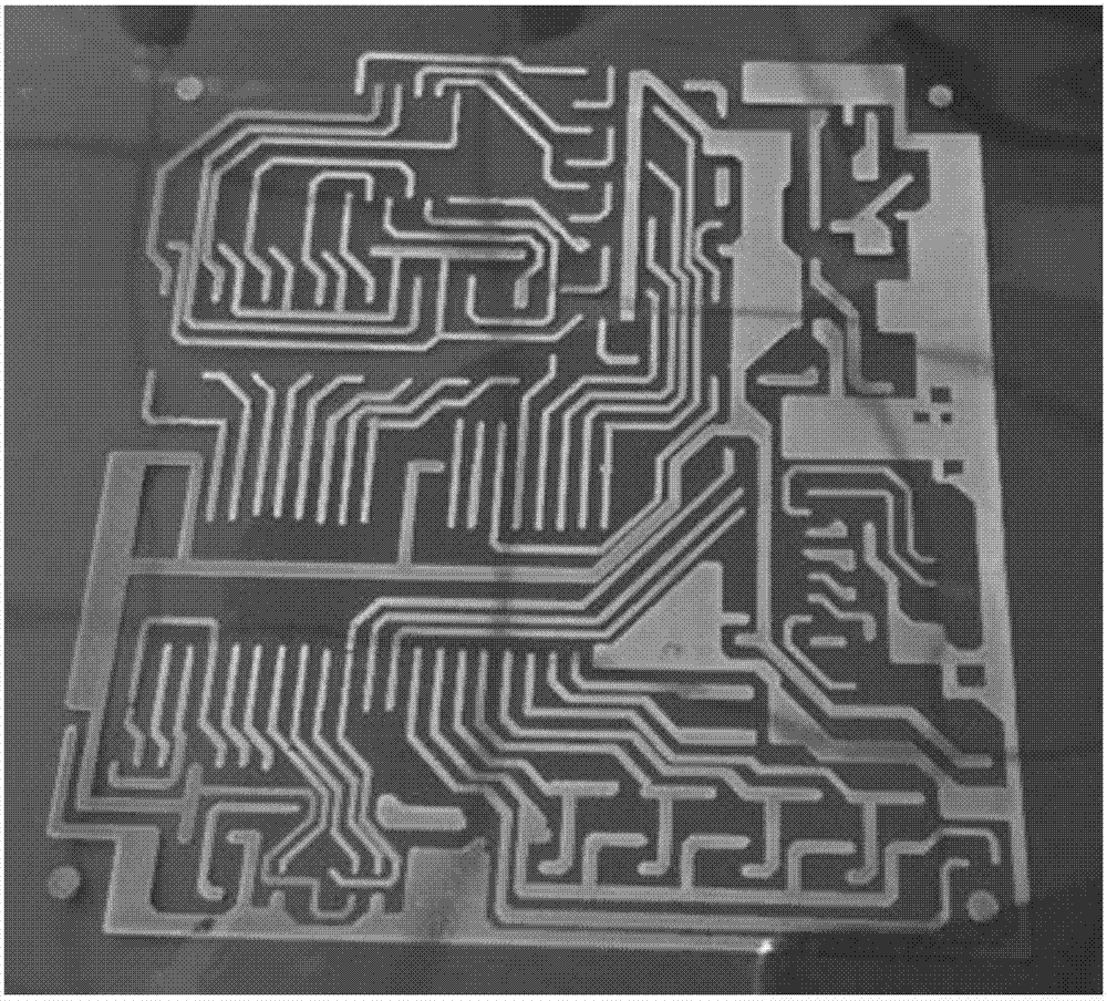
[0035] (3) Printing: Pd(NO) prepared in step (2) 3 ) 2 The ink is injected into the ink cartridge of the ME-10 type common inkjet printer, and the conductive circuit is printed on the base material processed through step (1), and it is naturally dried at room temperature after the printing is completed;
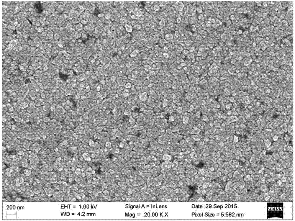
[0036] (4) Conductiv...
Embodiment 2
[0038] A conductive circuit printing process based on inkjet printing, comprising the following steps:
[0039] (1) Substrate pretreatment: Treat the acrylonitrile-butadiene-styrene plastic substrate with air plasma under the condition of air atmosphere and voltage of 200V for 8min, and then treat the acrylonitrile-butadiene-styrene plastic substrate at room temperature Put the plastic substrate into the ethanol solution of 10wt% silane coupling agent and soak for 24 hours, rinse the acrylonitrile-butadiene-styrene plastic substrate with ethanol and dry it for later use;
[0040] (2) Ink preparation: use deionized water and ethanol with a volume ratio of 2:1 as solvents to prepare AgNO with a concentration of 60mmol / L 3 ink;
[0041] (3) Printing: the AgNO prepared in step (2) 3 The ink is injected into the ink cartridge of the ME-10 type common inkjet printer, and the conductive circuit is printed on the base material processed through step (1), and it is naturally dried at r...
Embodiment 3
[0044] A conductive circuit printing process based on inkjet printing, comprising the following steps:
[0045] (1) Substrate pretreatment: treat the polyimide substrate with air plasma for 8 minutes under the condition of air atmosphere and voltage of 150V, then put the polyimide substrate into a concentration of 3wt% silane disulfide at room temperature Soak in the ethanol solution of the joint agent for 12h, rinse the polyimide substrate with ethanol and dry it for later use;
[0046] (2) Ink preparation: use deionized water and ethanol with a volume ratio of 1:10 as solvents to prepare AgNO with a concentration of 30mmol / L 3 ink;
[0047] (3) Printing: the AgNO prepared in step (2) 3 The ink is injected into the ink cartridge of the ME-10 type common inkjet printer, and the conductive circuit is printed on the base material processed through step (1), and it is naturally dried at room temperature after the printing is completed;
[0048] (4) Conductive pattern forming: ...
PUM
 Abstract
Description
Claims
Application Information
 - R&D
- Intellectual Property
- Life Sciences
- Materials
- Tech Scout
- Unparalleled Data Quality
- Higher Quality Content
- 60% Fewer Hallucinations
Browse by: Latest US Patents, China's latest patents, Technical Efficacy Thesaurus, Application Domain, Technology Topic, Popular Technical Reports.
© 2025 PatSnap. All rights reserved.Legal|Privacy policy|Modern Slavery Act Transparency Statement|Sitemap|About US| Contact US: help@patsnap.com