Chemical method for preparing halogenation methylamine lead photoelectric thin film in large-area manner

A halogenated methylamine, photoelectric thin film technology, applied in metal material coating process, coating, solid-state diffusion coating and other directions, can solve problems such as difficulty in large-area preparation, achieve a wide range of laboratory device research and industrial application prospects, overcome the The effect of demanding requirements and short response time

Active Publication Date: 2017-10-13
XUCHANG UNIV
View PDF1 Cites 4 Cited by
  • Summary
  • Abstract
  • Description
  • Claims
  • Application Information

AI Technical Summary

Problems solved by technology

[0005] The problem to be solved by the present invention is to provide a chemical method for preparing a large-area methylamine halide photoelectric thin film in view of the difficulties in large-area preparation in the preparation method of the lead methylamine halide thin film reported in the prior art.

Method used


Image

  • Chemical method for preparing halogenation methylamine lead photoelectric thin film in large-area manner
  • Chemical method for preparing halogenation methylamine lead photoelectric thin film in large-area manner
  • Chemical method for preparing halogenation methylamine lead photoelectric thin film in large-area manner

Examples


Embodiment 1

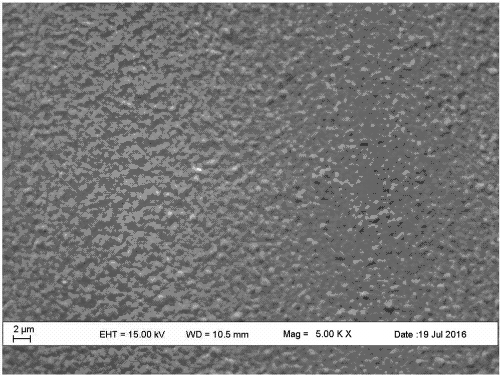
[0041] 1. Preparatory work: Sputter a 60nm-thick elemental lead film on the surface of a clean base material, and the film thickness is controlled by film thickness monitoring. Lead film area is 6cm 2 , the total mass of lead is about 0.41mg. The elemental lead thin film is ready for use after deposition.

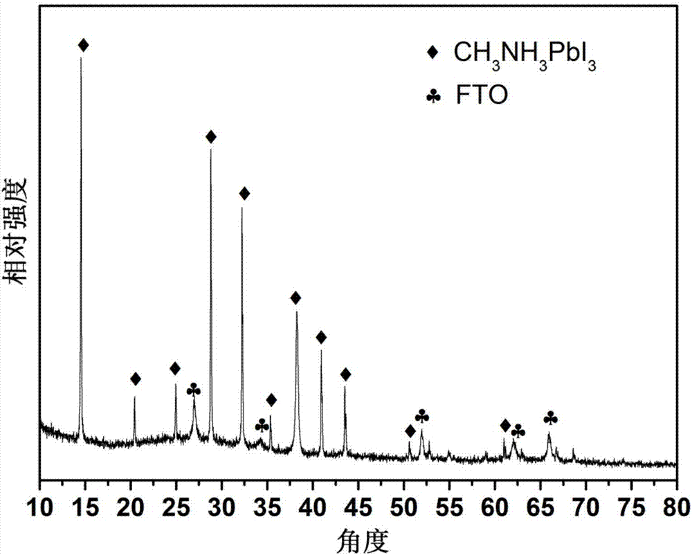
[0042]2. Reaction steps: Weigh 43 mg of methylamine iodide and place it in a crucible, place the substrate sputtered with lead elemental substance on top of the methylamine iodide powder and cover the crucible lid, and use an oil pump to evacuate the tube furnace to 0.01Mpa , and then feed nitrogen, repeat the operation 3 times, then vacuumize, and heat up under the vacuum condition of 0.01Mpa. Heating at 200°C for 50 min, and cooling to room temperature naturally with the furnace after the reaction is complete. Nitrogen gas was introduced to normal pressure, and the prepared methylamine halide lead film was taken out. SEM photo see figure 1 , XRD picture see figure ...

Embodiment 2

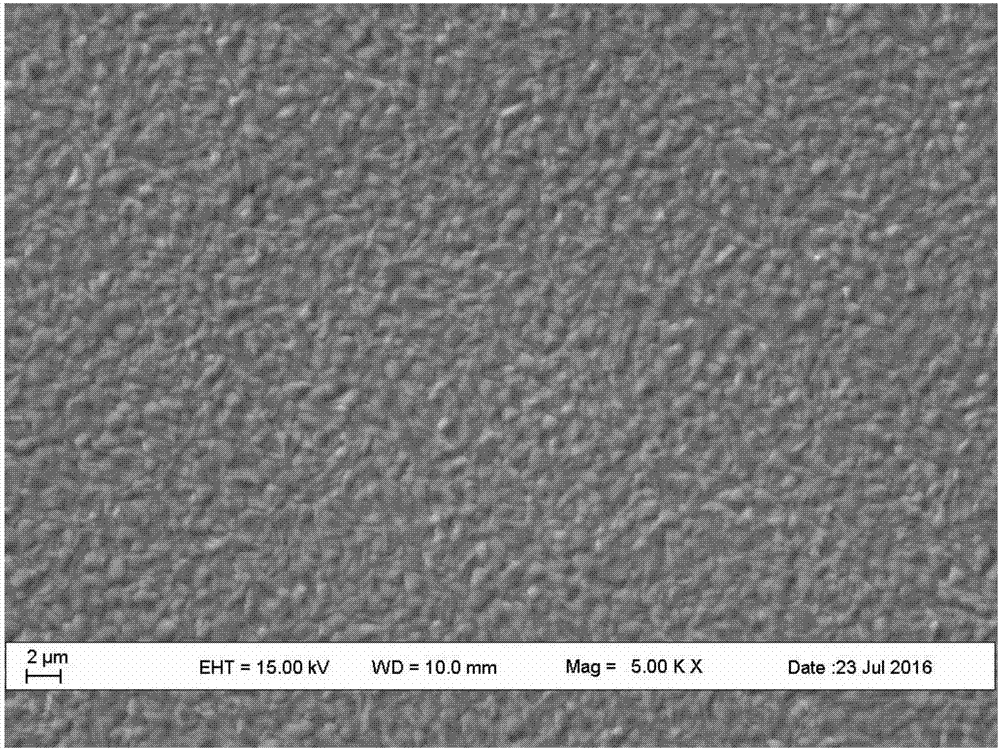
[0044] 1. Preparatory work: Sputter a 60nm-thick elemental lead film on the surface of a clean base material, and the film thickness is controlled by film thickness monitoring. Lead film area is 6cm 2 , the total mass of lead is about 0.41mg. The elemental lead thin film is ready for use after deposition.

[0045] 2. Reaction steps: Weigh 30 mg of methylamine iodide and place it in a crucible, place the substrate sputtered with lead elemental substance on top of the methylamine iodide powder and cover the crucible lid, and use an oil pump to evacuate the tube furnace to 0.01Mpa , and then feed nitrogen, repeat the operation 3 times, then vacuumize, and heat up under the vacuum condition of 0.01Mpa. Heat at 270°C for 3 minutes, and cool down to room temperature naturally with the furnace after the reaction is complete. Nitrogen gas was introduced to normal pressure, and the prepared methylamine halide lead film was taken out. SEM photo see image 3 , XRD picture see Figu...

Embodiment 3

[0047] 1. Preparatory work: Sputter a 50nm-thick elemental lead film on the surface of a clean base material, and the film thickness is controlled by film thickness monitoring. Lead film area is 6cm 2 , the total mass of lead is about 0.34mg. The elemental lead thin film is ready for use after deposition.

[0048] 2. Reaction steps: Weigh 40 mg of methylamine iodide and place it in a crucible, place the substrate sputtered with lead elemental substance on top of the methylamine iodide powder and cover the crucible lid, and use an oil pump to evacuate the tube furnace to 0.01Mpa , Then feed nitrogen, repeat this operation 3 times, then heat up under the vacuum condition of 0.01Mpa. Heat at 270°C for 3 minutes, and cool down to room temperature naturally with the furnace after the reaction is complete. Nitrogen gas was introduced to normal pressure, and the prepared methylamine halide lead film was taken out. SEM photo see Figure 5 , XRD picture see Figure 6 .


PUM

PropertyMeasurementUnit
thicknessaaaaaaaaaa
areaaaaaaaaaaa
diameteraaaaaaaaaa

Abstract

The invention relates to a chemical method for preparing a halogenation methylamine lead photoelectric thin film in a large-area manner. The method comprises the steps that a substrate deposited with a simple substance lead thin film and halogenation methylamine are heated under the vacuum or negative pressure condition, a reaction vessel is filled with halogenation methylamine, under the condition at the temperature of 200 DEG C to 300 DED C, the reaction is carried out, the reaction time is smaller than or equal to 50 min, and the halogenation methylamine lead semiconductor thin film material CH3NH3PbX3 with the large grain, good crystallinity and the uniform surface is prepared on the surface of the substrate material in an original manner, X is equal to Cl, Br, I or combination of one or two. According to the method, the halogenation methylamine lead thin film can be rapidly prepared in the large-area manner, the prepared halogenation methylamine lead thin film is good in thickness uniformity, halogenation methylamine lead is good in crystal and large in crystal size, the diameter can reach 0.5 to 2 micrometers, preferably, the diameter can reach one to three micrometers, the problem that in the traditional method, the film formation grain is small is solved, and the method has the wide experiment device research and industrial application prospect.

Description

Technical field: [0001] The invention belongs to the technical field of material chemistry, and in particular relates to a chemical method for preparing a large-area methylamine halide lead photoelectric thin film. Background technique: [0002] Lead methylamine halide (CH 3 NH 3 wxya 3 , X=Cl, Br, I) is a semiconductor material with a narrow bandgap of about 1.5eV. It has excellent photoelectric conversion capability and is widely used in the development of low-cost solar cell devices. The heterojunction thin-film solar cell device based on this material has achieved a photoelectric conversion efficiency as high as 22% in the laboratory. [0003] At present, the widely used synthesis methods of lead methylamine iodide thin films can be classified into two kinds, which are one-step method and two-step method. Among them, the solution-based "one-step" lead halide perovskite material solar cell is to dissolve the lead source and methyl halide ammonium salt or its derivativ...

Claims


Application Information

Patent Timeline
Patent Type & Authority Applications(China)
IPC IPC(8): C23C8/06
CPCC23C8/06
Inventor 雷岩谷龙艳张磊磊郑直杨晓刚高远浩铁伟伟
Owner XUCHANG UNIV
Why Eureka
Try Eureka