Manufacturing method for novel flexible thermoelectric element
A technology of thermoelectric elements and manufacturing methods, which is applied in the manufacture/processing of thermoelectric devices, thermoelectric device components, thermoelectric device node lead-out materials, etc., which can solve the problems that cannot be made into flexible thermoelectric devices on a large scale, and achieve energy density High, simple manufacturing process, compact circuit structure
- Summary
- Abstract
- Description
- Claims
- Application Information
AI Technical Summary
Problems solved by technology
Method used
Image

Examples
Embodiment 1
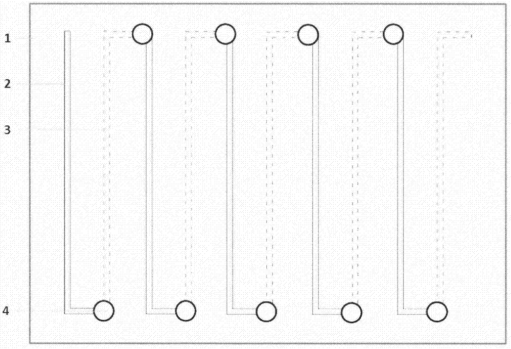
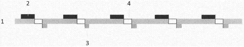
[0020] Preparation of carbon material filled poly-3,4 ethylenedioxythiophene: P-type thermoelectric material dispersion slurry of polysulfonated styrene and tungsten carbide filled poly-3,4 ethylenedioxythiophene / polydiallyl di The N-type thermoelectric material dispersion slurry of methyl ammonium chloride is used to print the P-type thermoelectric material slurry and the N-type thermoelectric material slurry on both sides of the flexible polyimide substrate respectively, and the N-type thermoelectric material slurry is obtained after drying And the circuit layer of P-type thermoelectric material, drill a row of through holes at both ends of the flexible insulating substrate, gold-plated in the through holes, and the circuit layers on both sides are connected through the gold-plated through holes at both ends to form an alternate series circuit structure of N-P-N-P... The flexible thermoelectric element is obtained, the front and cross-section are respectively as figure 1 wit...
Embodiment 2
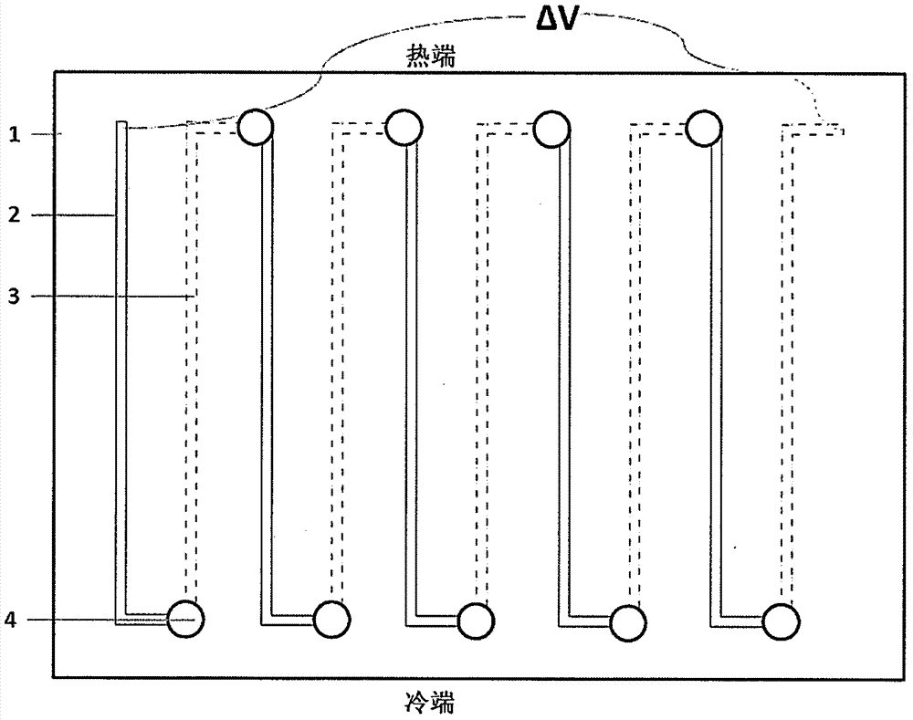
[0023] Prepare Bi 0.5 Sb 1.5 Te 3 P-type thermoelectric material dispersion slurry filled with polyvinylidene fluoride and Bi 2 Te 2.7 Se 0.3 N-type thermoelectric material dispersion slurry filled with polyvinylidene fluoride, printed P-type thermoelectric material slurry and N-type thermoelectric material slurry on both sides of the flexible polyethylene terephthalate substrate by screen printing, and dried Finally, the circuit layers of N-type and P-type thermoelectric materials are respectively obtained, and a row of through holes are drilled at both ends of the flexible insulating substrate, and silver is plated in the through holes, and the circuit layers on both sides are connected through the silver-plated through holes at both ends to form N-P-N-P ... the alternating series circuit structure to obtain flexible thermoelectric elements.
[0024] Dangru Figure 4 When current is passed through the series circuit shown, one side of the flexible substrate can be cool...
Embodiment 3
[0026] Prepare P-type thermoelectric material dispersion slurry filled with carbon nanotubes polyaniline and N-type thermoelectric material dispersion slurry filled with tungsten carbide polyvinylidene fluoride, and use screen printing on both sides of the flexible polybutylene terephthalate substrate Print P-type thermoelectric material slurry and N-type thermoelectric material slurry, and obtain circuit layers of N-type and P-type thermoelectric materials respectively after drying, and drill a row of through holes at both ends of the flexible insulating substrate. Copper plating, the circuit layers on both sides are connected through the copper-plated through-holes at both ends to form an alternating series circuit structure of N-P-N-P..., and a flexible thermoelectric element is obtained.
[0027] When there is a temperature difference between the two ends of the flexible insulating substrate, a potential difference is generated in the alternating series circuit structure, w...
PUM
| Property | Measurement | Unit |
|---|---|---|
| Power factor | aaaaa | aaaaa |
Abstract
Description
Claims
Application Information
 - Generate Ideas
- Intellectual Property
- Life Sciences
- Materials
- Tech Scout
- Unparalleled Data Quality
- Higher Quality Content
- 60% Fewer Hallucinations
Browse by: Latest US Patents, China's latest patents, Technical Efficacy Thesaurus, Application Domain, Technology Topic, Popular Technical Reports.
© 2025 PatSnap. All rights reserved.Legal|Privacy policy|Modern Slavery Act Transparency Statement|Sitemap|About US| Contact US: help@patsnap.com