Texturizing method for monocrystalline silicon wafer and texturizing additive used in texturizing method

A technology of silicon silicon wafers and additives, which is applied in the field of monocrystalline silicon wafer texturing methods and its texturing additives, can solve the problems of slow alkali etching silicon wafers, reduce production costs, and low production efficiency, and achieve silicon etching The effect of increasing sheet speed, reducing production cost, and improving production efficiency

Inactive Publication Date: 2017-11-10
JIA XING SHANGNENG PHOTOVOLTAIC MATERIALS SCI & TECH CO LTD
View PDF13 Cites 24 Cited by
  • Summary
  • Abstract
  • Description
  • Claims
  • Application Information

AI Technical Summary

Problems solved by technology

However, the disadvantage of the above method is that the alkali etching speed of the silicon wafer is relatively slow, between 15-30min, the production efficiency is low, and it is not conducive to reducing the production cost

Method used


Image

  • Texturizing method for monocrystalline silicon wafer and texturizing additive used in texturizing method
  • Texturizing method for monocrystalline silicon wafer and texturizing additive used in texturizing method
  • Texturizing method for monocrystalline silicon wafer and texturizing additive used in texturizing method

Examples


Embodiment 1

[0031] The monocrystalline silicon wafer texturing method of the present invention is prepared according to the following steps:

[0032] 1) Put the damage layer of P-type mortar wire-cut single crystal silicon wafer with a size of 156mm×156mm and a thickness of 200±20μm into a HF solution with a mass fraction of 3% to remove SiO 2 layer, the cleaning time is 60 seconds, and the cleaning temperature is 20 °C; then use deionized water to clean for 3 times; dry the silicon wafer for use;

[0033] 2) Put the above-treated silicon wafer into a temperature of 0.0005mol / LAgNO 3 , 0.2mol / L H2O2, 2 mol / L HF solution for 120s corrosion, the reaction temperature is 20℃;

[0034] 3) Wash the silicon wafer after the above treatment in deionized water for 60s, and the cleaning temperature is 20℃;

[0035] 4) The above silicon wafer was reacted in 2%wt NaOH, 0.001%wt surfactant, and 0.02%wt soluble starch for 300s, and the reaction temperature was 60°C;

[0036] 5) Washing the above sili...

Embodiment 2

[0039] 1) Put the damaged layer of P-type diamond wire-cut single crystal silicon wafer with a size of 156mm×156mm and a thickness of 180±10μm into a HF solution with a mass fraction of 3% to remove SiO 2 layer, the cleaning time is 60 seconds, and the cleaning temperature is 20 °C; then use deionized water to clean for 3 times; dry the silicon wafer for use;

[0040] 2) Put the above-treated silicon wafer into a temperature of 0.0001mol / LAgNO 3 , 0.5mol / L H 2 O 2 , 5 mol / L HF solution for 180s corrosion, the reaction temperature is 20℃;

[0041] 3) Wash the silicon wafer after the above treatment in deionized water for 60s, and the cleaning temperature is 20℃;

[0042] 4) The above silicon wafer was reacted in a solution containing 2%wtKOH, 0.001%wt glucose, and 0.02%wt sodium acetate for 360s, and the reaction temperature was 60°C;

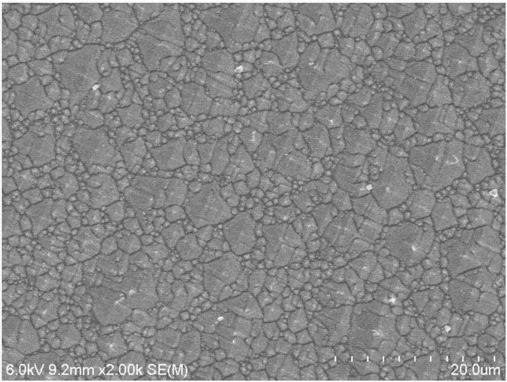
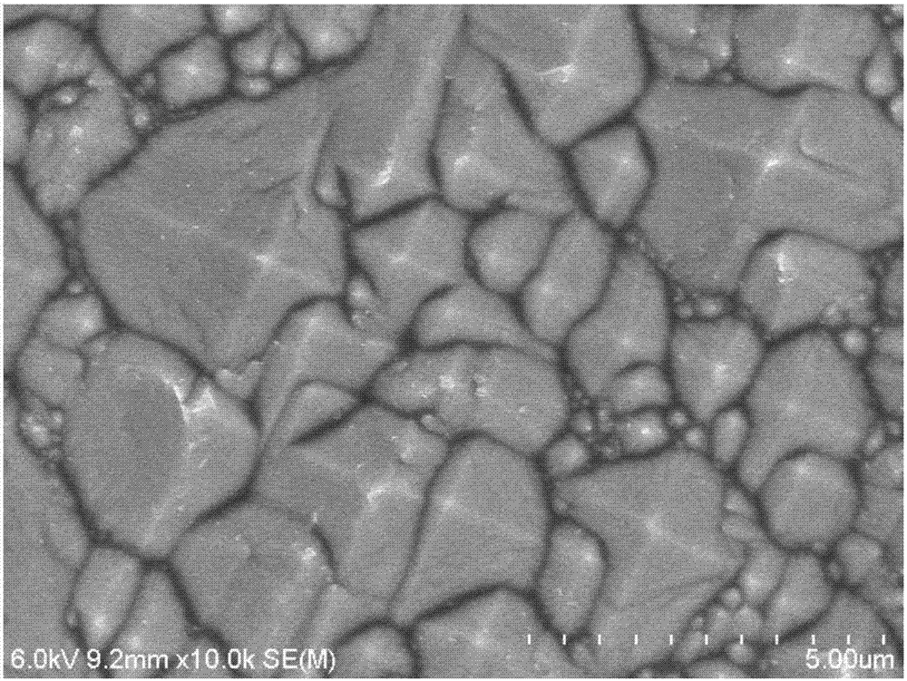
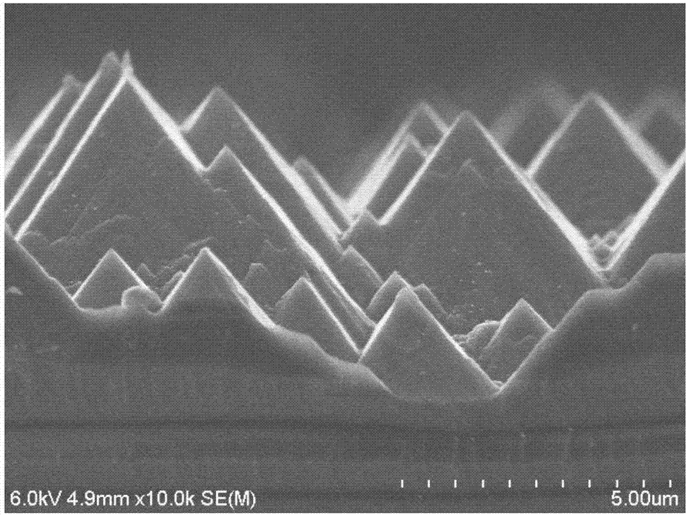
[0043] 5) Washing the above silicon wafer in deionized water and drying, the pyramid suede surface with excellent light trapping performanc...


PUM

PropertyMeasurementUnit
heightaaaaaaaaaa
reflectanceaaaaaaaaaa

Abstract

The invention discloses a texturizing method for a monocrystalline silicon wafer and a texturizing additive used in the texturizing method. The preparation method comprises the preparation steps as follows: 1) the silicon wafer is cleaned; 2) the silicon wafer is placed in a first chemical solution containing metal ions, an oxidizing agent and a chemical corrosive, and a nano structure texture is formed on the surface of the silicon wafer; 3) the silicon wafer is cleaned; 4) the silicon wafer is placed in a second chemical solution and a pyramid structure is formed through micro-chemical etching; 5) the silicon wafer is cleaned. The texturizing additive is any one or more of a surfactant, isopropanol, glucose, soluble starch and urea. Compared with preparation methods in the prior art, the preparation method of the crystalline silicon solar cell surface micro-nano structure has the benefits as follows: the etching rate is high; 2) the uniform pyramid structure is formed; 3) the surface light reflectivity of the prepared silicon wafer is 8%-12%; 4) the silicon wafer etching speed is greatly increased, the production efficiency is improved, and the production cost is reduced.

Description

technical field [0001] The invention relates to the field of photovoltaic technology, in particular to a single crystal silicon wafer texturing method and a texturing additive thereof. Background technique [0002] The mainstream power generation technology in today's photovoltaic field is to use crystalline silicon solar cells to generate electricity, mainly including monocrystalline silicon solar cells and polycrystalline silicon solar cells. Monocrystalline silicon solar cells account for about 30% of the market share of the photovoltaic industry. The most significant advantage is that the photoelectric conversion efficiency is high. The disadvantage is that the production cost is high and the production efficiency is low. The slicing technology of monocrystalline silicon is divided into mortar wire cutting technology and diamond wire cutting technology. Using diamond wire cutting technology to cut monocrystalline silicon wafers can reduce silicon consumption and improve ...

Claims


Application Information

Patent Timeline
Patent Type & Authority Applications(China)
IPC IPC(8): C30B33/10C30B29/06
CPCC30B29/06C30B33/10
Inventor 苏晓东胡奋琴
Owner JIA XING SHANGNENG PHOTOVOLTAIC MATERIALS SCI & TECH CO LTD
Why Eureka
Try Eureka