
GaN heterojunction longitudinal field effect transistor

A technology of field effect transistors and heterojunctions, applied in electrical components, circuits, semiconductor devices, etc., can solve the problems of low hole mobility of P-type GaN, increased parasitic capacitance and parasitic inductance, increased system volume and cost, etc. Achieve short reverse recovery time, low turn-on voltage, improve efficiency and stability

Active Publication Date: 2017-11-24
UNIV OF ELECTRONIC SCI & TECH OF CHINA
View PDF7 Cites 6 Cited by
  • Summary
  • Abstract
  • Description
  • Claims
  • Application Information

AI Technical Summary

Problems solved by technology

However, discrete freewheeling diodes not only increase the size and cost of the system, but also increase the parasitic capacitance and parasitic inductance, resulting in increased switching losses
Traditional GaN PN junction diodes are not suitable for use as freewheeling diodes due to their high turn-on voltage and low hole mobility of P-type GaN.

Method used


Image

  • GaN heterojunction longitudinal field effect transistor
  • GaN heterojunction longitudinal field effect transistor
  • GaN heterojunction longitudinal field effect transistor

Examples


Embodiment Construction

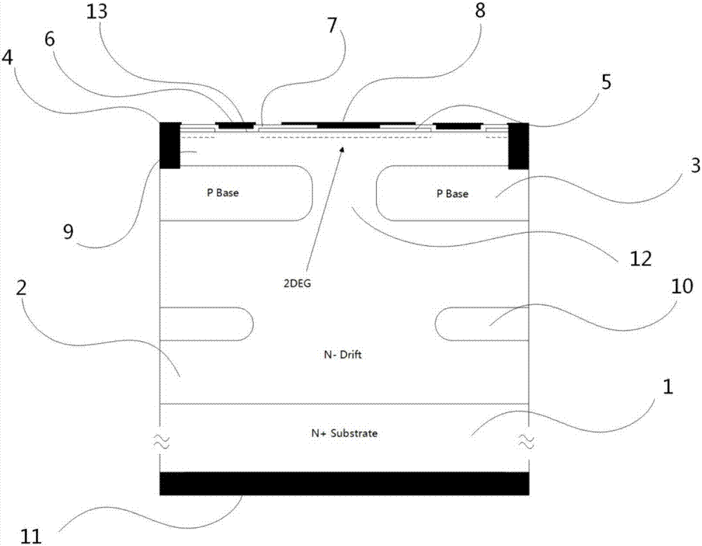
[0023] Below in conjunction with accompanying drawing, describe technical scheme of the present invention in detail:

[0024] The present invention proposes a high-performance GaN heterojunction reverse conduction field effect transistor. Different from the traditional transverse field effect transistor, the present invention adopts a vertical discrete gate structure and deposits a Schottky source between the two gates. The invention reduces the concentration of two-dimensional electron gas (2DEG) in the channel by etching the AlMN barrier layer and the P-type base region so that the device has a higher threshold voltage. Since the device adopts a vertical structure and has a floating P region, the electric field distribution is much more uniform than that of a traditional lateral device, which enables the device to achieve high withstand voltage and low on-resistance while saving wafer area. In the reverse conduction working state, the turn-on voltage of the Schottky diode of...


PUM

PropertyMeasurementUnit
Thicknessaaaaaaaaaa
Depthaaaaaaaaaa

Abstract

The invention relates to the technical field of a semiconductor device, and relates to a GaN heterojunction longitudinal field effect transistor. The GaN heterojunction longitudinal field effect transistor is characterized in that a longitudinal discrete grating structure is utilized, and a schottky source electrode is deposited between grids to form an anode of a reverse conducting diode; by introducing back barriers and grooved gates formed in P type base regions, the two dimensional electron gas (2DEG) at the channel below the gate is used up through the combined action of the back barriers and the grooved gates, and the threshold-voltage can be accurately regulated and controlled by adjusting the etching thickness of an AlMN barrier layer. In the working state of a forward direction switch, the GaN heterojunction longitudinal field effect transistor has the advantages of being adjustable in the threshold-voltage, being low in the conduction resistance, being large in the saturation current, being high in the off state withstand voltage, being high in the working frequency and being low in power consumption. In the reverse conducting state, the GaN heterojunction longitudinal field effect transistor has the advantages of being low in the starting voltage, being low in the conduction resistance, being high in the reverse withstand voltage, being short in the reverse recovery time and being low in power consumption. And at the same time, the manufacturing technique of the GaN heterojunction longitudinal field effect transistor is compatible with a traditional GaN heterojunction HEMT device. The GaN heterojunction longitudinal field effect transistor is especially suitable for a GaN heterojunction longitudinal power field effect transistor.

Description

technical field [0001] The invention relates to the technical field of semiconductor devices, and relates to a GaN heterojunction power field effect transistor. Background technique [0002] As a typical representative of the third-generation wide-bandgap semiconductor, gallium nitride (GaN) has many excellent characteristics: high critical breakdown electric field (~3.5×10 6 V / cm), high electron mobility (~2000cm 2 / vs), high two-dimensional electron gas (2DEG) concentration (~10 13 cm -2 ) and good high temperature working ability, etc. High electron mobility transistor (HEMT) based on AlGaN / GaN heterojunction (or heterojunction field effect transistor HFET, modulation doped field effect transistor MODFET, hereinafter collectively referred to as HEMT devices) has been used in wireless communication, satellite communication and other radio frequency / Microwave field. In addition, such devices based on wide-bandgap GaN materials have the characteristics of high off-stat...

Claims


Application Information

Patent Timeline
IPC IPC(8): H01L29/06H01L29/10H01L29/423H01L29/47H01L29/778
CPCH01L29/0684H01L29/1037H01L29/4236H01L29/475H01L29/7788
Inventor 周琦朱若璞陈万军张波
Owner UNIV OF ELECTRONIC SCI & TECH OF CHINA
Learn More